

21
Substrate-Induced Strain Engineering in CMOS Technology
2.3 Strained SiGe:C Film Growth
Heteroepitaxial SiGe:C layers have attracted serious attention as a material
for performance boost in the state-of-the-art MOSFET devices during recent
years. Alloying silicon with germanium and carbon adds exclusive opportunities for strain and band gap engineering. The growth of SiGe:C alloys
on Si is a challenging task in the sense of finding suitable source materials
and growth conditions for a ternary alloy. It is important to investigate the
Fully strained Si 1–x Ge x
(a)
(b)
(c)
Fully relaxed Si substrate
Fully relaxed Si substrate
Fully or partially relaxed
Si 1–x Ge x
Partially strained Si 1–x Ge x
Fully strained Si 1–x Ge x
Fully relaxed Si substrate
Partially or fully relaxed
Si 1–x Ge x
Misfit dislocations
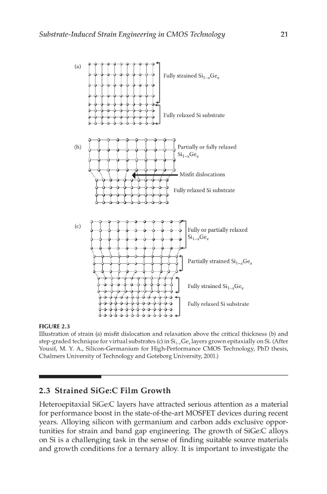
FIGURE 2.3
Illustration of strain (a) misfit dislocation and relaxation above the critical thickness (b) and
step-graded technique for virtual substrates (c) in Si 1–x Ge x layers grown epitaxially on Si. (After
Yousif, M. Y. A., Silicon-Germanium for High-Performance CMOS Technology, PhD thesis,
Chalmers University of Technology and Goteborg University, 2001.)
Substrate-Induced Strain Engineering in CMOS Technology
2.3 Strained SiGe:C Film Growth
Heteroepitaxial SiGe:C layers have attracted serious attention as a material
for performance boost in the state-of-the-art MOSFET devices during recent
years. Alloying silicon with germanium and carbon adds exclusive opportunities for strain and band gap engineering. The growth of SiGe:C alloys
on Si is a challenging task in the sense of finding suitable source materials
and growth conditions for a ternary alloy. It is important to investigate the
Fully strained Si 1–x Ge x
(a)
(b)
(c)
Fully relaxed Si substrate
Fully relaxed Si substrate
Fully or partially relaxed
Si 1–x Ge x
Partially strained Si 1–x Ge x
Fully strained Si 1–x Ge x
Fully relaxed Si substrate
Partially or fully relaxed
Si 1–x Ge x
Misfit dislocations
FIGURE 2.3
Illustration of strain (a) misfit dislocation and relaxation above the critical thickness (b) and
step-graded technique for virtual substrates (c) in Si 1–x Ge x layers grown epitaxially on Si. (After
Yousif, M. Y. A., Silicon-Germanium for High-Performance CMOS Technology, PhD thesis,
Chalmers University of Technology and Goteborg University, 2001.)