

9
Introduction
process modelling, and it is one of the few enabling methodologies that can
reduce circuit development cycle time and cost. As the mainstream CMOS
technology is scaled into the nanometer regime, development of a rigorous
physical and predictive compact model for circuit simulation that covers
geometry, bias, temperature, DC, AC, RF, and noise characteristics becomes
a major challenge. Compact models have been at the heart of CAD tools for
circuit design over the past decades, and are playing an ever increasingly
important role in semiconductor manufacturing. Development of a compact
model describing a new technology is essential prior to the adoption of the
technology by the semiconductor industry. TCAD is currently being used for
process and device design, manufacturing, and yield improvement.
Traditionally, a custom design is considered superior because it delivers higher performance and smaller die size, thus resulting in lower cost;
however, this results in a longer design cycle (time to market) and is now
a serious challenge for the 22 nm CMOS technology node and beyond. It
is expected that the future of designs in 22 nm and beyond will be system
design with design automation at all levels. Statistical fluctuations inherent in any IC manufacturing process cause variations in device and hence
in circuit performance. Thus, product yield and manufacturing problems
Defect effect on
device/circuit
Full TCAD Flow
Process effect
on device/circuit
Process variations
Materials
Process
Device
Circuit
Gate
Block
Process/structural variations
Parameter extraction
Technology
development
Transistor optimisation
System performance
Analog/digital
design
Subcircuit expansion
Compact model (BSIM, PSP, PCM)
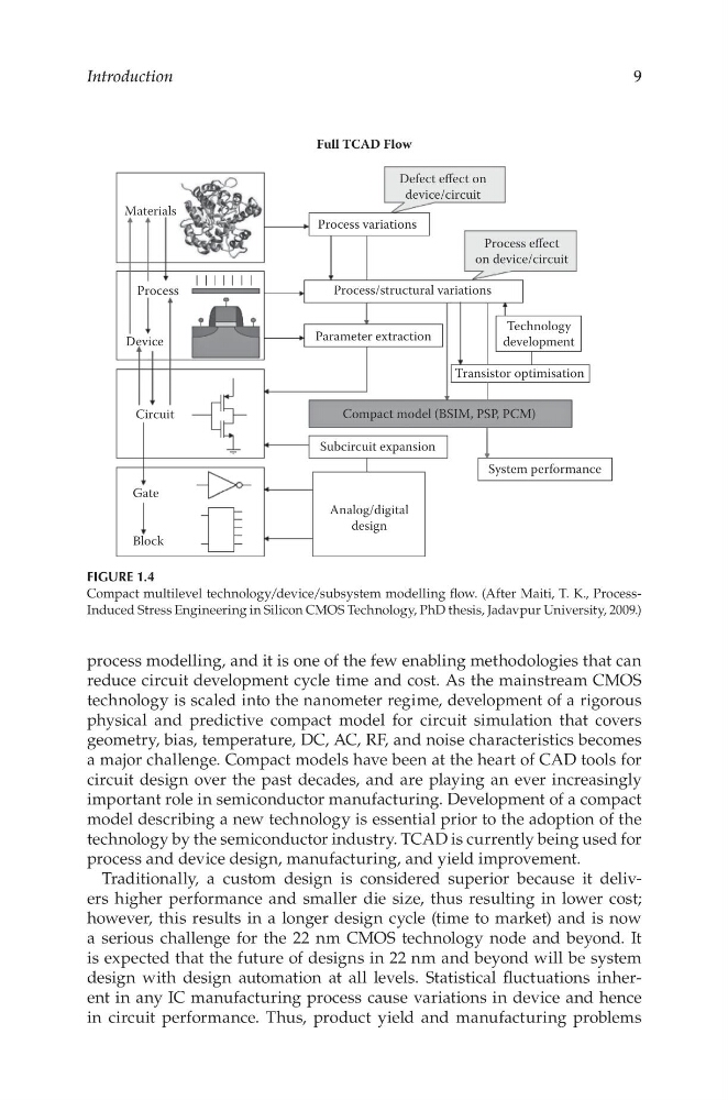
FIGURE 1.4
Compact multilevel technology/device/subsystem modelling flow. (After Maiti, T. K., ProcessInduced Stress Engineering in Silicon CMOS Technology, PhD thesis, Jadavpur University, 2009.)
Introduction
process modelling, and it is one of the few enabling methodologies that can
reduce circuit development cycle time and cost. As the mainstream CMOS
technology is scaled into the nanometer regime, development of a rigorous
physical and predictive compact model for circuit simulation that covers
geometry, bias, temperature, DC, AC, RF, and noise characteristics becomes
a major challenge. Compact models have been at the heart of CAD tools for
circuit design over the past decades, and are playing an ever increasingly
important role in semiconductor manufacturing. Development of a compact
model describing a new technology is essential prior to the adoption of the
technology by the semiconductor industry. TCAD is currently being used for
process and device design, manufacturing, and yield improvement.
Traditionally, a custom design is considered superior because it delivers higher performance and smaller die size, thus resulting in lower cost;
however, this results in a longer design cycle (time to market) and is now
a serious challenge for the 22 nm CMOS technology node and beyond. It
is expected that the future of designs in 22 nm and beyond will be system
design with design automation at all levels. Statistical fluctuations inherent in any IC manufacturing process cause variations in device and hence
in circuit performance. Thus, product yield and manufacturing problems
Defect effect on
device/circuit
Full TCAD Flow
Process effect
on device/circuit
Process variations
Materials
Process
Device
Circuit
Gate
Block
Process/structural variations
Parameter extraction
Technology
development
Transistor optimisation
System performance
Analog/digital
design
Subcircuit expansion
Compact model (BSIM, PSP, PCM)
FIGURE 1.4
Compact multilevel technology/device/subsystem modelling flow. (After Maiti, T. K., ProcessInduced Stress Engineering in Silicon CMOS Technology, PhD thesis, Jadavpur University, 2009.)