

283
Process-Aware Design of Strain-Engineered MOSFETs
L g (nm)
170
Ge (cm
–2 )
1.62e+22
1.5e+22
4e+08
–0.007
0.001
6.15e–05
–0.00112
–0.000358
–0.428
–3.73e+09
1.27e+21
2.5e+21
–2.1e+09
–0.245
1.23e–09
–10
35
125
StressXX (Pa)
2.03e+09
V t (V)
0.176
I off (A/um)
0.00136
G m (S/um)
0.00246
(a)
PSS p-MOSFET
0.00128
L g (nm)
200
SiN (nm)
0.089
0.085
6.7e+08
0.439
0.004
0.00333
0.000178
–0.00238
–0.00252
–0.171
–8.41e+08
0.041
0.045
8.73e+06
0.016
8.49e–05
–40
35
125
StressXX (Pa)
1.52e+09
V t (V)
0.627
ID max (A/um)
0.00661
G m (S/um)
0.00589
(b)
PSS n–MOSFET
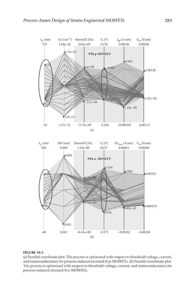
FIGURE 10.5
(a) Parallel coordinate plot. The process is optimised with respect to threshold voltage, current,
and transconductance for process-induced strained Si p-MOSFETs. (b) Parallel coordinate plot.
The process is optimised with respect to threshold voltage, current, and transconductance for
process-induced strained Si n-MOSFETs.
Process-Aware Design of Strain-Engineered MOSFETs
L g (nm)
170
Ge (cm
–2 )
1.62e+22
1.5e+22
4e+08
–0.007
0.001
6.15e–05
–0.00112
–0.000358
–0.428
–3.73e+09
1.27e+21
2.5e+21
–2.1e+09
–0.245
1.23e–09
–10
35
125
StressXX (Pa)
2.03e+09
V t (V)
0.176
I off (A/um)
0.00136
G m (S/um)
0.00246
(a)
PSS p-MOSFET
0.00128
L g (nm)
200
SiN (nm)
0.089
0.085
6.7e+08
0.439
0.004
0.00333
0.000178
–0.00238
–0.00252
–0.171
–8.41e+08
0.041
0.045
8.73e+06
0.016
8.49e–05
–40
35
125
StressXX (Pa)
1.52e+09
V t (V)
0.627
ID max (A/um)
0.00661
G m (S/um)
0.00589
(b)
PSS n–MOSFET
FIGURE 10.5
(a) Parallel coordinate plot. The process is optimised with respect to threshold voltage, current,
and transconductance for process-induced strained Si p-MOSFETs. (b) Parallel coordinate plot.
The process is optimised with respect to threshold voltage, current, and transconductance for
process-induced strained Si n-MOSFETs.