

278
Strain-Engineered MOSFETs
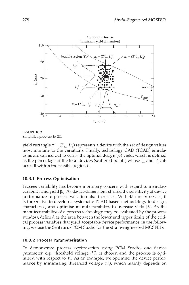
yield rectangle x c = (T c ox , L c g ) represents a device with the set of design values
most immune to the variations. Finally, technology CAD (TCAD) simulations are carried out to verify the optimal design (x c ) yield, which is defined
as the percentage of the total devices (scattered points) whose I on and V t values fall within the feasible region F c .
10.3.1 Process Optimisation
Process variability has become a primary concern with regard to manufacturability and yield [5]. As device dimensions shrink, the sensitivity of device
performance to process variation also increases. With 45 nm processes, it
is imperative to develop a systematic TCAD-based methodology to design,
characterise, and optimise manufacturability to increase yield [6]. As the
manufacturability of a process technology may be evaluated by the process
window, defined as the area between the lower and upper limits of the critical process variables that yield acceptable device performance, in the following, we use the Sentaurus PCM Studio for the strain-engineered MOSFETs.
10.3.2 Process Parameterisation
To demonstrate process optimisation using PCM Studio, one device
parameter, e.g., threshold voltage (V t ), is chosen and the process is optimised with respect to V t . As an example, we optimise the device performance by minimising threshold voltage (V t ), which mainly depends on
110
Optimum Device
(maximum yield dimension)
90
70
L
g (nm)
50
30
1.3
1.4
1.5
1.6
1.7
T ox (nm)
1.8
1.9
2.0
2.1
x l = (T
l ox , L
l g ) T ox
l
L g
l
L g
u
x c = (T
c
ox, L
c
g )
x u = (T
u ox, L
u
g )
T ox
u
V tmax
I onmax
Feasible region (F c )
FIGURE 10.2
Simplified problem in 2D.
Strain-Engineered MOSFETs
yield rectangle x c = (T c ox , L c g ) represents a device with the set of design values
most immune to the variations. Finally, technology CAD (TCAD) simulations are carried out to verify the optimal design (x c ) yield, which is defined
as the percentage of the total devices (scattered points) whose I on and V t values fall within the feasible region F c .
10.3.1 Process Optimisation
Process variability has become a primary concern with regard to manufacturability and yield [5]. As device dimensions shrink, the sensitivity of device
performance to process variation also increases. With 45 nm processes, it
is imperative to develop a systematic TCAD-based methodology to design,
characterise, and optimise manufacturability to increase yield [6]. As the
manufacturability of a process technology may be evaluated by the process
window, defined as the area between the lower and upper limits of the critical process variables that yield acceptable device performance, in the following, we use the Sentaurus PCM Studio for the strain-engineered MOSFETs.
10.3.2 Process Parameterisation
To demonstrate process optimisation using PCM Studio, one device
parameter, e.g., threshold voltage (V t ), is chosen and the process is optimised with respect to V t . As an example, we optimise the device performance by minimising threshold voltage (V t ), which mainly depends on
110
Optimum Device
(maximum yield dimension)
90
70
L
g (nm)
50
30
1.3
1.4
1.5
1.6
1.7
T ox (nm)
1.8
1.9
2.0
2.1
x l = (T
l ox , L
l g ) T ox
l
L g
l
L g
u
x c = (T
c
ox, L
c
g )
x u = (T
u ox, L
u
g )
T ox
u
V tmax
I onmax
Feasible region (F c )
FIGURE 10.2
Simplified problem in 2D.