

279
Process-Aware Design of Strain-Engineered MOSFETs
the following parameters: halo implant dose (Halo_Dose) and extension
implant dose (Ext_Dose), gate length (L g ), gate oxide thickness (G ox ), and
peak temperature for rapid thermal annealing (RTA), which modifies the
doping concentration in the channel region. The optimisation problem
consists of finding the best combination of the above parameters that produces the desired threshold voltage. The visual optimisation procedure
[7] allows one to put constraints on the input parameters, which, however,
are motivated by the manufacturing considerations. For an example, we
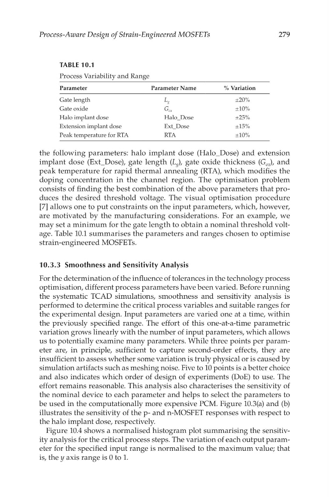
may set a minimum for the gate length to obtain a nominal threshold voltage. Table 10.1 summarises the parameters and ranges chosen to optimise
strain-engineered MOSFETs.
10.3.3 Smoothness and Sensitivity Analysis
For the determination of the influence of tolerances in the technology process
optimisation, different process parameters have been varied. Before running
the systematic TCAD simulations, smoothness and sensitivity analysis is
performed to determine the critical process variables and suitable ranges for
the experimental design. Input parameters are varied one at a time, within
the previously specified range. The effort of this one-at-a-time parametric
variation grows linearly with the number of input parameters, which allows
us to potentially examine many parameters. While three points per parameter are, in principle, sufficient to capture second-order effects, they are
insufficient to assess whether some variation is truly physical or is caused by
simulation artifacts such as meshing noise. Five to 10 points is a better choice
and also indicates which order of design of experiments (DoE) to use. The
effort remains reasonable. This analysis also characterises the sensitivity of
the nominal device to each parameter and helps to select the parameters to
be used in the computationally more expensive PCM. Figure 10.3(a) and (b)
illustrates the sensitivity of the p- and n-MOSFET responses with respect to
the halo implant dose, respectively.
Figure 10.4 shows a normalised histogram plot summarising the sensitivity analysis for the critical process steps. The variation of each output parameter for the specified input range is normalised to the maximum value; that
is, the y axis range is 0 to 1.
TABLE 10.1
Process Variability and Range
Parameter
Parameter Name
% Variation
Gate length
L g
±20%
Gate oxide
G ox
±10%
Halo implant dose
Halo_Dose
±25%
Extension implant dose
Ext_Dose
±15%
Peak temperature for RTA
RTA
±10%
Process-Aware Design of Strain-Engineered MOSFETs
the following parameters: halo implant dose (Halo_Dose) and extension
implant dose (Ext_Dose), gate length (L g ), gate oxide thickness (G ox ), and
peak temperature for rapid thermal annealing (RTA), which modifies the
doping concentration in the channel region. The optimisation problem
consists of finding the best combination of the above parameters that produces the desired threshold voltage. The visual optimisation procedure
[7] allows one to put constraints on the input parameters, which, however,
are motivated by the manufacturing considerations. For an example, we
may set a minimum for the gate length to obtain a nominal threshold voltage. Table 10.1 summarises the parameters and ranges chosen to optimise
strain-engineered MOSFETs.
10.3.3 Smoothness and Sensitivity Analysis
For the determination of the influence of tolerances in the technology process
optimisation, different process parameters have been varied. Before running
the systematic TCAD simulations, smoothness and sensitivity analysis is
performed to determine the critical process variables and suitable ranges for
the experimental design. Input parameters are varied one at a time, within
the previously specified range. The effort of this one-at-a-time parametric
variation grows linearly with the number of input parameters, which allows
us to potentially examine many parameters. While three points per parameter are, in principle, sufficient to capture second-order effects, they are
insufficient to assess whether some variation is truly physical or is caused by
simulation artifacts such as meshing noise. Five to 10 points is a better choice
and also indicates which order of design of experiments (DoE) to use. The
effort remains reasonable. This analysis also characterises the sensitivity of
the nominal device to each parameter and helps to select the parameters to
be used in the computationally more expensive PCM. Figure 10.3(a) and (b)
illustrates the sensitivity of the p- and n-MOSFET responses with respect to
the halo implant dose, respectively.
Figure 10.4 shows a normalised histogram plot summarising the sensitivity analysis for the critical process steps. The variation of each output parameter for the specified input range is normalised to the maximum value; that
is, the y axis range is 0 to 1.
TABLE 10.1
Process Variability and Range
Parameter
Parameter Name
% Variation
Gate length
L g
±20%
Gate oxide
G ox
±10%
Halo implant dose
Halo_Dose
±25%
Extension implant dose
Ext_Dose
±15%
Peak temperature for RTA
RTA
±10%