

276
Strain-Engineered MOSFETs
scales, for example, optical interference effects, result in intradie variation.
In advanced CMOS technologies, intradie variation is comparable to and in
some cases significantly larger than interdie variation. A further classification distinguishes between systematic variation and random variation.
Systematic variation is attributed to known and predictable phenomena.
Examples include optical proximity effects, layout-induced stress, and the
well proximity effect. Optical proximity effects have received a great deal
of attention in recent years, with optical proximity emerging as a common
technique to mitigate these effects. The partial compensation of systematic
variation in the process and design phases afforded by these types of tools
provides more tolerance for technology scaling. Random variation, on the
other hand, is due to inherently unpredictable fluctuations of the manufacturing process. It cannot be controlled with standard statistical process control (SPC) techniques, making it difficult or expensive to minimise. Examples
include fluctuations in channel doping, gate oxide thickness, and gate length.
Some studies indicate random variation could have the largest impact on chip
yield in future, highly scaled, CMOS technologies. Manufacturing-induced
variation can be thoroughly characterised and decomposed into several
deterministic components, including wafer-to-wafer variation, across-wafer
variation, within-die variation, and pattern-dependent variation. Wafer-towafer variation arises from variation in the state of the manufacturing tool.
Over time, the conditions of a given process may drift so that wafers passing
through a given process step near the beginning of a lot undergo a slightly
different process than those processed near the end. Typically sources of
wafer-to-wafer variation exist in process steps, such as the etch and chemical mechanical polishing (CMP) modules; however, due to major advances
in factory quality control, principally through automated statistical process
control, wafer-to-wafer variation can be considered a lesser source of concern than across-wafer variation.
Variation
Extrinsic
Intrinsic
Random
Equipment
Litho
C MP
Etch
Stress
EM
Device
Reliability
Physics
Systematic
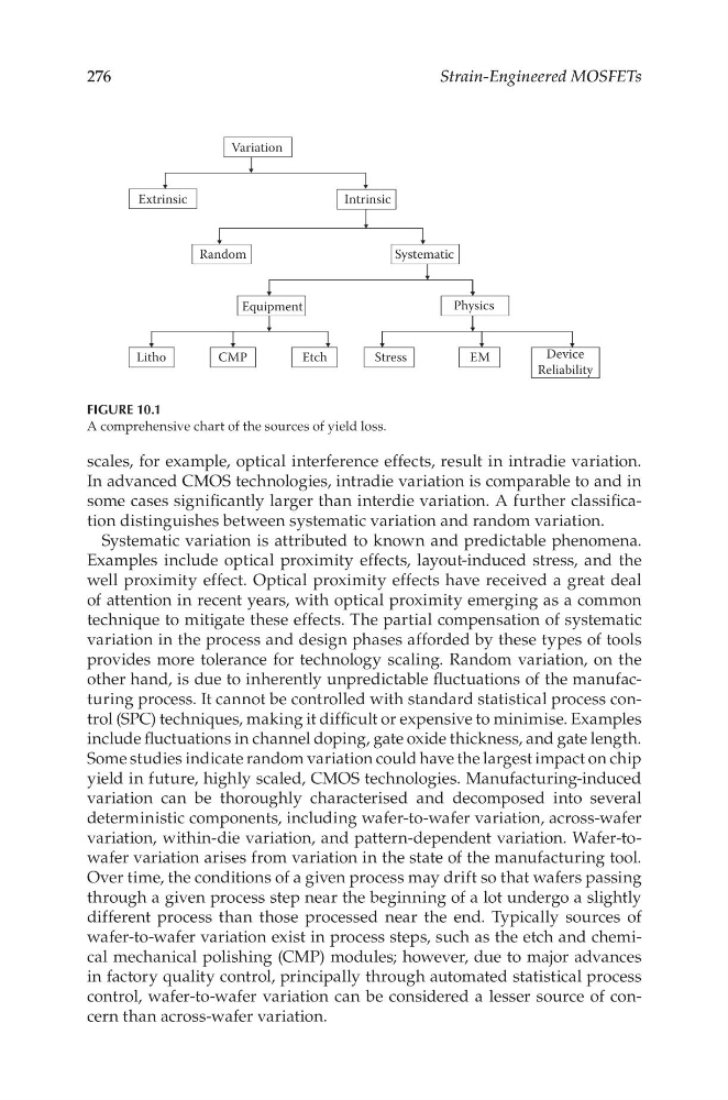
FIGURE 10.1
A comprehensive chart of the sources of yield loss.
Strain-Engineered MOSFETs
scales, for example, optical interference effects, result in intradie variation.
In advanced CMOS technologies, intradie variation is comparable to and in
some cases significantly larger than interdie variation. A further classification distinguishes between systematic variation and random variation.
Systematic variation is attributed to known and predictable phenomena.
Examples include optical proximity effects, layout-induced stress, and the
well proximity effect. Optical proximity effects have received a great deal
of attention in recent years, with optical proximity emerging as a common
technique to mitigate these effects. The partial compensation of systematic
variation in the process and design phases afforded by these types of tools
provides more tolerance for technology scaling. Random variation, on the
other hand, is due to inherently unpredictable fluctuations of the manufacturing process. It cannot be controlled with standard statistical process control (SPC) techniques, making it difficult or expensive to minimise. Examples
include fluctuations in channel doping, gate oxide thickness, and gate length.
Some studies indicate random variation could have the largest impact on chip
yield in future, highly scaled, CMOS technologies. Manufacturing-induced
variation can be thoroughly characterised and decomposed into several
deterministic components, including wafer-to-wafer variation, across-wafer
variation, within-die variation, and pattern-dependent variation. Wafer-towafer variation arises from variation in the state of the manufacturing tool.
Over time, the conditions of a given process may drift so that wafers passing
through a given process step near the beginning of a lot undergo a slightly
different process than those processed near the end. Typically sources of
wafer-to-wafer variation exist in process steps, such as the etch and chemical mechanical polishing (CMP) modules; however, due to major advances
in factory quality control, principally through automated statistical process
control, wafer-to-wafer variation can be considered a lesser source of concern than across-wafer variation.
Variation
Extrinsic
Intrinsic
Random
Equipment
Litho
C MP
Etch
Stress
EM
Device
Reliability
Physics
Systematic
FIGURE 10.1
A comprehensive chart of the sources of yield loss.