

268
Strain-Engineered MOSFETs
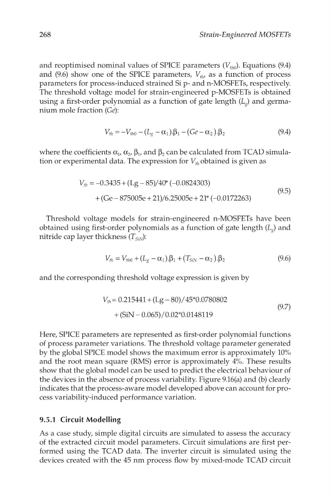
and reoptimised nominal values of SPICE parameters (V th0 ). Equations (9.4)
and (9.6) show one of the SPICE parameters, V th , as a function of process
parameters for process-induced strained Si p- and n-MOSFETs, respectively.
The threshold voltage model for strain-engineered p-MOSFETs is obtained
using a first-order polynomial as a function of gate length (L g ) and germanium mole fraction (Ge):
V
V
L
G e
(
) .
.
th
th
g
0
1
1
2
2
(
)
= −
−
−α β −
−α β
(9.4)
where the coefficients α 1 , α 2 , β 1 , and β 2 can be calculated from TCAD simulation or experimental data. The expression for V th obtained is given as
= −
+
−
−
+
−
+
+
−
V th
0.3435 (Lg 85)/40* ( 0.0824303)
(Ge 875005e 21)/6.25005e 21* ( 0.0172263)
(9.5)
Threshold voltage models for strain-engineered n-MOSFETs have been
obtained using first-order polynomials as a function of gate length (L g ) and
nitride cap layer thickness (T SiN ):
V V
L
T
(
) .
.
th
th
g
S iN
0
1
1
2
2
(
)
=
+
− α β +
− α β
(9.6)
and the corresponding threshold voltage expression is given by
V = 0.215441 (Lg 80)/45*0.0780802
(SiN 0.065)/0.02*0.0148119
th
+
−
+
−
(9.7)
Here, SPICE parameters are represented as first-order polynomial functions
of process parameter variations. The threshold voltage parameter generated
by the global SPICE model shows the maximum error is approximately 10%
and the root mean square (RMS) error is approximately 4%. These results
show that the global model can be used to predict the electrical behaviour of
the devices in the absence of process variability. Figure 9.16(a) and (b) clearly
indicates that the process-aware model developed above can account for process variability-induced performance variation.
9.5.1 Circuit Modelling
As a case study, simple digital circuits are simulated to assess the accuracy
of the extracted circuit model parameters. Circuit simulations are first performed using the TCAD data. The inverter circuit is simulated using the
devices created with the 45 nm process flow by mixed-mode TCAD circuit
Strain-Engineered MOSFETs
and reoptimised nominal values of SPICE parameters (V th0 ). Equations (9.4)
and (9.6) show one of the SPICE parameters, V th , as a function of process
parameters for process-induced strained Si p- and n-MOSFETs, respectively.
The threshold voltage model for strain-engineered p-MOSFETs is obtained
using a first-order polynomial as a function of gate length (L g ) and germanium mole fraction (Ge):
V
V
L
G e
(
) .
.
th
th
g
0
1
1
2
2
(
)
= −
−
−α β −
−α β
(9.4)
where the coefficients α 1 , α 2 , β 1 , and β 2 can be calculated from TCAD simulation or experimental data. The expression for V th obtained is given as
= −
+
−
−
+
−
+
+
−
V th
0.3435 (Lg 85)/40* ( 0.0824303)
(Ge 875005e 21)/6.25005e 21* ( 0.0172263)
(9.5)
Threshold voltage models for strain-engineered n-MOSFETs have been
obtained using first-order polynomials as a function of gate length (L g ) and
nitride cap layer thickness (T SiN ):
V V
L
T
(
) .
.
th
th
g
S iN
0
1
1
2
2
(
)
=
+
− α β +
− α β
(9.6)
and the corresponding threshold voltage expression is given by
V = 0.215441 (Lg 80)/45*0.0780802
(SiN 0.065)/0.02*0.0148119
th
+
−
+
−
(9.7)
Here, SPICE parameters are represented as first-order polynomial functions
of process parameter variations. The threshold voltage parameter generated
by the global SPICE model shows the maximum error is approximately 10%
and the root mean square (RMS) error is approximately 4%. These results
show that the global model can be used to predict the electrical behaviour of
the devices in the absence of process variability. Figure 9.16(a) and (b) clearly
indicates that the process-aware model developed above can account for process variability-induced performance variation.
9.5.1 Circuit Modelling
As a case study, simple digital circuits are simulated to assess the accuracy
of the extracted circuit model parameters. Circuit simulations are first performed using the TCAD data. The inverter circuit is simulated using the
devices created with the 45 nm process flow by mixed-mode TCAD circuit