

255
Process Compact Modelling of Strain-Engineered MOSFETs
V th behaviour of short-channel transistors, drain-induced barrier lowering (DIBL) needs to be accounted for. To the first order, this effect is captured by E ta0 , which is a model parameter for the DIBL effect. Its value is
extracted from published data of V th roll-off, and the trend of E ta0 is illustrated in Figure 9.6.
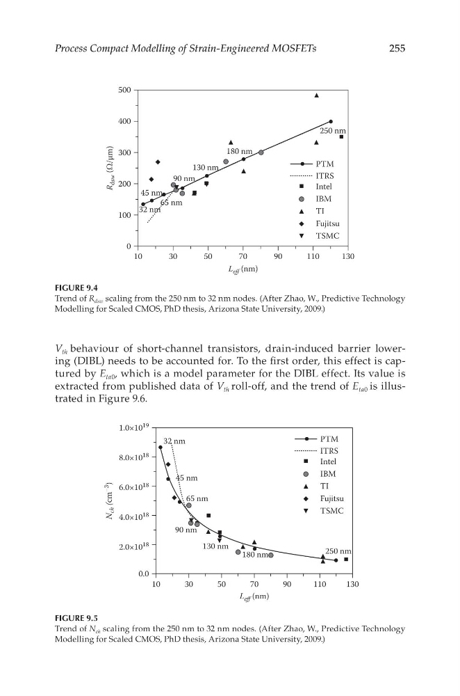
FIGURE 9.4
Trend of R dsw scaling from the 250 nm to 32 nm nodes. (After Zhao, W., Predictive Technology
Modelling for Scaled CMOS, PhD thesis, Arizona State University, 2009.)
1.0×10
19
8.0×10
18
6.0×10
18
4.0×10
18
2.0×10
18
0.0
10
30
50
70
L eff (nm)
90
110
130
N
ch (cm
–3
)
32 nm
45 nm
65 nm
90 nm
130 nm
180 nm
250 nm
PTM
ITRS
Intel
IBM
TI
Fujitsu
TSMC
FIGURE 9.5
Trend of N ch scaling from the 250 nm to 32 nm nodes. (After Zhao, W., Predictive Technology
Modelling for Scaled CMOS, PhD thesis, Arizona State University, 2009.)
Process Compact Modelling of Strain-Engineered MOSFETs
V th behaviour of short-channel transistors, drain-induced barrier lowering (DIBL) needs to be accounted for. To the first order, this effect is captured by E ta0 , which is a model parameter for the DIBL effect. Its value is
extracted from published data of V th roll-off, and the trend of E ta0 is illustrated in Figure 9.6.
FIGURE 9.4
Trend of R dsw scaling from the 250 nm to 32 nm nodes. (After Zhao, W., Predictive Technology
Modelling for Scaled CMOS, PhD thesis, Arizona State University, 2009.)
1.0×10
19
8.0×10
18
6.0×10
18
4.0×10
18
2.0×10
18
0.0
10
30
50
70
L eff (nm)
90
110
130
N
ch (cm
–3
)
32 nm
45 nm
65 nm
90 nm
130 nm
180 nm
250 nm
PTM
ITRS
Intel
IBM
TI
Fujitsu
TSMC
FIGURE 9.5
Trend of N ch scaling from the 250 nm to 32 nm nodes. (After Zhao, W., Predictive Technology
Modelling for Scaled CMOS, PhD thesis, Arizona State University, 2009.)