

254
Strain-Engineered MOSFETs
details of a transistor. In particular, channel doping concentration, N ch , is
mainly defined by the threshold voltage. The exact value of N ch is reversed
from published data of V th0 , using the V th model in BSIM [4]. Figure 9.5
illustrates the trend of N ch scaling. Based on N ch , the main coefficient for
the body effect of V th , K 1 , is also estimated. Furthermore, to model the
130 nm
180 nm
250 nm
PTM
Intel
IBM
TI
Fujitsu
TSMC
90 nm
65 nm
32 nm
45 nm
4.5
4.0
3.5
3.0
2.5
2.0
1.5
1.0
0.5
0.0
10
30
50
70
L eff (nm)
90
110
130
EOT (nm)
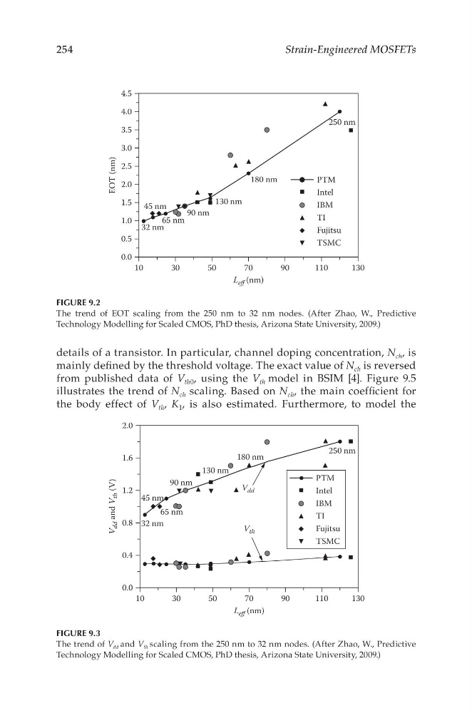
FIGURE 9.2
The trend of EOT scaling from the 250 nm to 32 nm nodes. (After Zhao, W., Predictive
Technology Modelling for Scaled CMOS, PhD thesis, Arizona State University, 2009.)
130 nm
180 nm
V dd
V th
250 nm
PTM
Intel
IBM
TI
Fujitsu
TSMC
90 nm
65 nm
45 nm
32 nm
2.0
1.6
1.2
0.8
0.4
0.0
10
30
50
70
L eff (nm)
90
110
130
V
dd and V
th (V)
FIGURE 9.3
The trend of V dd and V th scaling from the 250 nm to 32 nm nodes. (After Zhao, W., Predictive
Technology Modelling for Scaled CMOS, PhD thesis, Arizona State University, 2009.)
Strain-Engineered MOSFETs
details of a transistor. In particular, channel doping concentration, N ch , is
mainly defined by the threshold voltage. The exact value of N ch is reversed
from published data of V th0 , using the V th model in BSIM [4]. Figure 9.5
illustrates the trend of N ch scaling. Based on N ch , the main coefficient for
the body effect of V th , K 1 , is also estimated. Furthermore, to model the
130 nm
180 nm
250 nm
PTM
Intel
IBM
TI
Fujitsu
TSMC
90 nm
65 nm
32 nm
45 nm
4.5
4.0
3.5
3.0
2.5
2.0
1.5
1.0
0.5
0.0
10
30
50
70
L eff (nm)
90
110
130
EOT (nm)
FIGURE 9.2
The trend of EOT scaling from the 250 nm to 32 nm nodes. (After Zhao, W., Predictive
Technology Modelling for Scaled CMOS, PhD thesis, Arizona State University, 2009.)
130 nm
180 nm
V dd
V th
250 nm
PTM
Intel
IBM
TI
Fujitsu
TSMC
90 nm
65 nm
45 nm
32 nm
2.0
1.6
1.2
0.8
0.4
0.0
10
30
50
70
L eff (nm)
90
110
130
V
dd and V
th (V)
FIGURE 9.3
The trend of V dd and V th scaling from the 250 nm to 32 nm nodes. (After Zhao, W., Predictive
Technology Modelling for Scaled CMOS, PhD thesis, Arizona State University, 2009.)