

243
Reliability and Degradation of Strain-Engineered MOSFETs
different process sequences were studied for SiGe S/D, changing the step
sequence of junction formation and selectively epitaxial growth (SEG).
Interrupted NBTI measurements were complemented in this study with
charge pumping and noise measurements in order to obtain a more complete
view of defects present and their generation under stress. The effects of the
processing steps on electrical properties of the devices were carefully taken
into account, allowing us to make a fair comparison between devices with
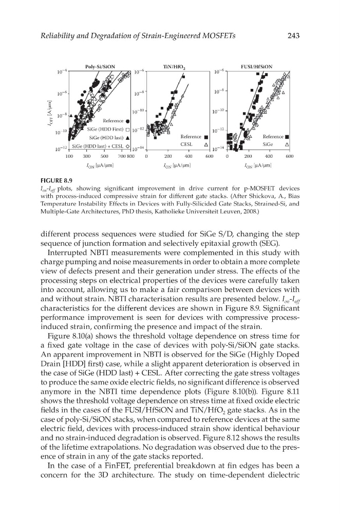
and without strain. NBTI characterisation results are presented below. I on -I off
characteristics for the different devices are shown in Figure 8.9. Significant
performance improvement is seen for devices with compressive processinduced strain, confirming the presence and impact of the strain.
Figure 8.10(a) shows the threshold voltage dependence on stress time for
a fixed gate voltage in the case of devices with poly-Si/SiON gate stacks.
An apparent improvement in NBTI is observed for the SiGe (Highly Doped
Drain [HDD] first) case, while a slight apparent deterioration is observed in
the case of SiGe (HDD last) + CESL. After correcting the gate stress voltages
to produce the same oxide electric fields, no significant difference is observed
anymore in the NBTI time dependence plots (Figure 8.10(b)). Figure 8.11
shows the threshold voltage dependence on stress time at fixed oxide electric
fields in the cases of the FUSI/HfSiON and TiN/HfO 2 gate stacks. As in the
case of poly-Si/SiON stacks, when compared to reference devices at the same
electric field, devices with process-induced strain show identical behaviour
and no strain-induced degradation is observed. Figure 8.12 shows the results
of the lifetime extrapolations. No degradation was observed due to the presence of strain in any of the gate stacks reported.
In the case of a FinFET, preferential breakdown at fin edges has been a
concern for the 3D architecture. The study on time-dependent dielectric
Poly-Si/SiON
TiN/HfO 2
FUSI/Hf SiON
10
4
10
6
10
8
10
10
10
12
10
6
10
8
10
10
10
12
10
14
10
6
10
8
10
10
10
12
10
14
100
300
500
700 800
I
OFF [A/μm]
I ON [μA/μm]
0
200
400
Reference
CESL
Reference
SiGe (HDD First)
SiGe (HDD last)
SiGe (HDD last) + CESL
Reference
SiGe
600
I ON [μA/μm]
0
200
400
600
I ON [μA/μm]
FIGURE 8.9
I on -I off plots, showing significant improvement in drive current for p-MOSFET devices
with process-induced compressive strain for different gate stacks. (After Shickova, A., Bias
Temperature Instability Effects in Devices with Fully-Silicided Gate Stacks, Strained-Si, and
Multiple-Gate Architectures, PhD thesis, Katholieke Universiteit Leuven, 2008.)
Reliability and Degradation of Strain-Engineered MOSFETs
different process sequences were studied for SiGe S/D, changing the step
sequence of junction formation and selectively epitaxial growth (SEG).
Interrupted NBTI measurements were complemented in this study with
charge pumping and noise measurements in order to obtain a more complete
view of defects present and their generation under stress. The effects of the
processing steps on electrical properties of the devices were carefully taken
into account, allowing us to make a fair comparison between devices with
and without strain. NBTI characterisation results are presented below. I on -I off
characteristics for the different devices are shown in Figure 8.9. Significant
performance improvement is seen for devices with compressive processinduced strain, confirming the presence and impact of the strain.
Figure 8.10(a) shows the threshold voltage dependence on stress time for
a fixed gate voltage in the case of devices with poly-Si/SiON gate stacks.
An apparent improvement in NBTI is observed for the SiGe (Highly Doped
Drain [HDD] first) case, while a slight apparent deterioration is observed in
the case of SiGe (HDD last) + CESL. After correcting the gate stress voltages
to produce the same oxide electric fields, no significant difference is observed
anymore in the NBTI time dependence plots (Figure 8.10(b)). Figure 8.11
shows the threshold voltage dependence on stress time at fixed oxide electric
fields in the cases of the FUSI/HfSiON and TiN/HfO 2 gate stacks. As in the
case of poly-Si/SiON stacks, when compared to reference devices at the same
electric field, devices with process-induced strain show identical behaviour
and no strain-induced degradation is observed. Figure 8.12 shows the results
of the lifetime extrapolations. No degradation was observed due to the presence of strain in any of the gate stacks reported.
In the case of a FinFET, preferential breakdown at fin edges has been a
concern for the 3D architecture. The study on time-dependent dielectric
Poly-Si/SiON
TiN/HfO 2
FUSI/Hf SiON
10
4
10
6
10
8
10
10
10
12
10
6
10
8
10
10
10
12
10
14
10
6
10
8
10
10
10
12
10
14
100
300
500
700 800
I
OFF [A/μm]
I ON [μA/μm]
0
200
400
Reference
CESL
Reference
SiGe (HDD First)
SiGe (HDD last)
SiGe (HDD last) + CESL
Reference
SiGe
600
I ON [μA/μm]
0
200
400
600
I ON [μA/μm]
FIGURE 8.9
I on -I off plots, showing significant improvement in drive current for p-MOSFET devices
with process-induced compressive strain for different gate stacks. (After Shickova, A., Bias
Temperature Instability Effects in Devices with Fully-Silicided Gate Stacks, Strained-Si, and
Multiple-Gate Architectures, PhD thesis, Katholieke Universiteit Leuven, 2008.)