

244
Strain-Engineered MOSFETs
10
–1
V G = –2.0 V
E OX = 8.2 MV/cm
ΔV th = At
b
b ~ 0.15 – 0.16
10
–2
10
–3
1
10
10
2
10
3
1
Stress Time [s]
Stress Time [s]
(a)
(b)
10
10
2
10
3
10
4
Reference
SiGe (HDD first)
SiGe (HDD last)
SiGe (HDD last) + CESL
ΔV
th [V]
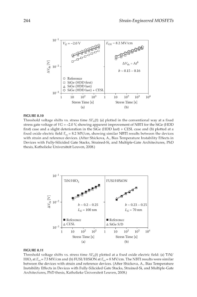
FIGURE 8.10
Threshold voltage shifts vs. stress time ΔV th (t): (a) plotted in the conventional way at a fixed
stress gate voltage of VG = –2.0 V, showing apparent improvement of NBTI for the SiGe (HDD
first) case and a slight deterioration in the SiGe (HDD last) + CESL case and (b) plotted at a
fixed oxide electric field E ox = 8.2 MV/cm, showing similar NBTI results between the devices
with strain and reference devices. (After Shickova, A., Bias Temperature Instability Effects in
Devices with Fully-Silicided Gate Stacks, Strained-Si, and Multiple-Gate Architectures, PhD
thesis, Katholieke Universiteit Leuven, 2008.)
1
10
–3
10
–2
10
–1
10
10
2
10
3
1
10
10
2
10
3
10
4
Stress Time [s]
Stress Time [s]
(a)
( b)
CESL
Reference
SiGe S/D
Reference
TiN/HfO 2
FUSI/HfSiON
b ~ 0.2 – 0.25
L G = 100 nm
b ~ 0.23 – 0.25
L G = 70 nm
ΔV
th [V]
FIGURE 8.11
Threshold voltage shifts vs. stress time ΔV th (t) plotted at a fixed oxide electric field: (a) TiN/
HfO 2 at E ox = 7.3 MV/cm and (b) FUSI/HfSiON at E ox = 8 MV/cm. The NBTI results were similar
between the devices with strain and reference devices. (After Shickova, A., Bias Temperature
Instability Effects in Devices with Fully-Silicided Gate Stacks, Strained-Si, and Multiple-Gate
Architectures, PhD thesis, Katholieke Universiteit Leuven, 2008.)
Strain-Engineered MOSFETs
10
–1
V G = –2.0 V
E OX = 8.2 MV/cm
ΔV th = At
b
b ~ 0.15 – 0.16
10
–2
10
–3
1
10
10
2
10
3
1
Stress Time [s]
Stress Time [s]
(a)
(b)
10
10
2
10
3
10
4
Reference
SiGe (HDD first)
SiGe (HDD last)
SiGe (HDD last) + CESL
ΔV
th [V]
FIGURE 8.10
Threshold voltage shifts vs. stress time ΔV th (t): (a) plotted in the conventional way at a fixed
stress gate voltage of VG = –2.0 V, showing apparent improvement of NBTI for the SiGe (HDD
first) case and a slight deterioration in the SiGe (HDD last) + CESL case and (b) plotted at a
fixed oxide electric field E ox = 8.2 MV/cm, showing similar NBTI results between the devices
with strain and reference devices. (After Shickova, A., Bias Temperature Instability Effects in
Devices with Fully-Silicided Gate Stacks, Strained-Si, and Multiple-Gate Architectures, PhD
thesis, Katholieke Universiteit Leuven, 2008.)
1
10
–3
10
–2
10
–1
10
10
2
10
3
1
10
10
2
10
3
10
4
Stress Time [s]
Stress Time [s]
(a)
( b)
CESL
Reference
SiGe S/D
Reference
TiN/HfO 2
FUSI/HfSiON
b ~ 0.2 – 0.25
L G = 100 nm
b ~ 0.23 – 0.25
L G = 70 nm
ΔV
th [V]
FIGURE 8.11
Threshold voltage shifts vs. stress time ΔV th (t) plotted at a fixed oxide electric field: (a) TiN/
HfO 2 at E ox = 7.3 MV/cm and (b) FUSI/HfSiON at E ox = 8 MV/cm. The NBTI results were similar
between the devices with strain and reference devices. (After Shickova, A., Bias Temperature
Instability Effects in Devices with Fully-Silicided Gate Stacks, Strained-Si, and Multiple-Gate
Architectures, PhD thesis, Katholieke Universiteit Leuven, 2008.)