

4
Strain-Engineered MOSFETs
processing steps and new materials. In 2005, the strategic research agenda
and vision for “more than Moore” technology had been formulated in a systematic manner by the European Technology Platform for Nanoelectronics.
1.1 Technology Scaling
In order to improve the speed of ULSI/GSI devices, new materials and device
structures are being proposed. Mobility enhancement techniques such as
global (substrate) strain and process-induced (local) stress are currently the
most promising for improving device performance. There are a number of
ways to induce strain in silicon. Different types of strain have distinct effects
on electron and hole mobilities. Starting from the 90 nm technology nodes,
advanced CMOS technologies feature multiple process-induced stressors
such as compressive and tensile overlayers, embedded SiGe, and multiple
stress memorisation techniques. Large magnitudes of uniaxial channel are
being incorporated in p-MOSFETs in the 65 nm technology node, and an
even higher stress level is required beyond the 22 nm technology node. Local
strain approaches are based on dedicated processing steps or process modules, such as shallow trench isolation, silicidation or metal gate electrodes, the
use of liners and capping layers, dry etch processes, contact etch stop layers,
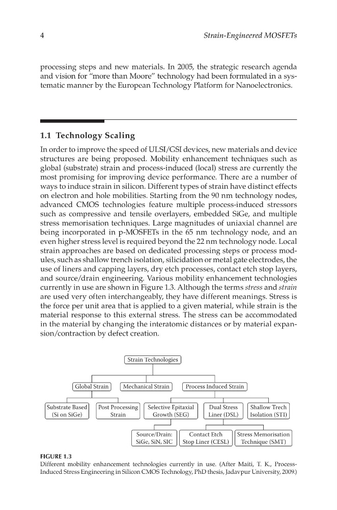
and source/drain engineering. Various mobility enhancement technologies
currently in use are shown in Figure 1.3. Although the terms stress and strain
are used very often interchangeably, they have different meanings. Stress is
the force per unit area that is applied to a given material, while strain is the
material response to this external stress. The stress can be accommodated
in the material by changing the interatomic distances or by material expansion/contraction by defect creation.
Strain Technologies
Global Strain
Substrate Based
(Si on SiGe)
Post Processing
Strain
Selective Epitaxial
Growth (SEG)
Source/Drain:
SiGe, SiN, SIC
Contact Etch
Stop Liner (CESL)
Stress Memorisation
Technique (SMT)
Dual Stress
Liner (DSL)
Shallow Trech
Isolation (STI)
Mechanical Strain
Process Induced Strain
FIGURE 1.3
Different mobility enhancement technologies currently in use. (After Maiti, T. K., ProcessInduced Stress Engineering in Silicon CMOS Technology, PhD thesis, Jadavpur University, 2009.)
Strain-Engineered MOSFETs
processing steps and new materials. In 2005, the strategic research agenda
and vision for “more than Moore” technology had been formulated in a systematic manner by the European Technology Platform for Nanoelectronics.
1.1 Technology Scaling
In order to improve the speed of ULSI/GSI devices, new materials and device
structures are being proposed. Mobility enhancement techniques such as
global (substrate) strain and process-induced (local) stress are currently the
most promising for improving device performance. There are a number of
ways to induce strain in silicon. Different types of strain have distinct effects
on electron and hole mobilities. Starting from the 90 nm technology nodes,
advanced CMOS technologies feature multiple process-induced stressors
such as compressive and tensile overlayers, embedded SiGe, and multiple
stress memorisation techniques. Large magnitudes of uniaxial channel are
being incorporated in p-MOSFETs in the 65 nm technology node, and an
even higher stress level is required beyond the 22 nm technology node. Local
strain approaches are based on dedicated processing steps or process modules, such as shallow trench isolation, silicidation or metal gate electrodes, the
use of liners and capping layers, dry etch processes, contact etch stop layers,
and source/drain engineering. Various mobility enhancement technologies
currently in use are shown in Figure 1.3. Although the terms stress and strain
are used very often interchangeably, they have different meanings. Stress is
the force per unit area that is applied to a given material, while strain is the
material response to this external stress. The stress can be accommodated
in the material by changing the interatomic distances or by material expansion/contraction by defect creation.
Strain Technologies
Global Strain
Substrate Based
(Si on SiGe)
Post Processing
Strain
Selective Epitaxial
Growth (SEG)
Source/Drain:
SiGe, SiN, SIC
Contact Etch
Stop Liner (CESL)
Stress Memorisation
Technique (SMT)
Dual Stress
Liner (DSL)
Shallow Trech
Isolation (STI)
Mechanical Strain
Process Induced Strain
FIGURE 1.3
Different mobility enhancement technologies currently in use. (After Maiti, T. K., ProcessInduced Stress Engineering in Silicon CMOS Technology, PhD thesis, Jadavpur University, 2009.)