

3
Introduction
forefront in addressing the challenges by successfully driving transistor
innovations from research phase to mainstream CMOS manufacturing.
Process-induced stress engineering has kept the expectations high when
Intel announced the tri-gate MOSFETs in 22 nm technology node in May
2011. The first 3D tri-gate transistor appearing at 22 nm will have a big
impact on the industry. It has been predicted that the tri-gate FinFETs are
both viable and capable of being tailored to suit the power/performance
trade-offs for a range of applications and exceed the capabilities of present silicon-on-insulator (SOI) technology. Tri-gate FinFETs built on high-k/
metal gate (HK-MG) technology, which will continue with Intel’s 22 nm
platform, have the flexibility for lower power consumption and much
higher performance.
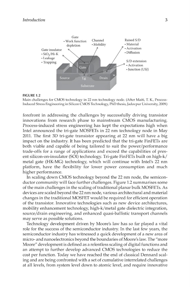
In scaling down CMOS technology beyond the 22 nm node, the semiconductor community will face further challenges. Figure 1.2 summarises some
of the main challenges in the scaling of traditional planar bulk MOSFETs. As
devices are scaled beyond the 22 nm node, various architectural and material
changes in the traditional MOSFET would be required for efficient operation
of the transistor. Innovative technologies such as new device architectures,
mobility enhancement technology, high-k/metal gate dielectric integration,
source/drain engineering, and enhanced quasi-ballistic transport channels
may serve as possible solutions.
Technology development driven by Moore’s law has so far played a vital
role for the success of the semiconductor industry. In the last few years, the
semiconductor industry has witnessed a quick development of a new area of
micro- and nanoelectronics beyond the boundaries of Moore’s law. The “more
Moore” development is defined as a relentless scaling of digital functions and
an attempt to further develop advanced CMOS technologies to reduce the
cost per function. Today we have reached the end of classical Dennard scaling and are being confronted with a set of cumulative interrelated challenges
at all levels, from system level down to atomic level, and require innovative
FIGURE 1.2
Main challenges for CMOS technology in 22 nm technology node. (After Maiti, T. K., ProcessInduced Stress Engineering in Silicon CMOS Technology, PhD thesis, Jadavpur University, 2009.)
Introduction
forefront in addressing the challenges by successfully driving transistor
innovations from research phase to mainstream CMOS manufacturing.
Process-induced stress engineering has kept the expectations high when
Intel announced the tri-gate MOSFETs in 22 nm technology node in May
2011. The first 3D tri-gate transistor appearing at 22 nm will have a big
impact on the industry. It has been predicted that the tri-gate FinFETs are
both viable and capable of being tailored to suit the power/performance
trade-offs for a range of applications and exceed the capabilities of present silicon-on-insulator (SOI) technology. Tri-gate FinFETs built on high-k/
metal gate (HK-MG) technology, which will continue with Intel’s 22 nm
platform, have the flexibility for lower power consumption and much
higher performance.
In scaling down CMOS technology beyond the 22 nm node, the semiconductor community will face further challenges. Figure 1.2 summarises some
of the main challenges in the scaling of traditional planar bulk MOSFETs. As
devices are scaled beyond the 22 nm node, various architectural and material
changes in the traditional MOSFET would be required for efficient operation
of the transistor. Innovative technologies such as new device architectures,
mobility enhancement technology, high-k/metal gate dielectric integration,
source/drain engineering, and enhanced quasi-ballistic transport channels
may serve as possible solutions.
Technology development driven by Moore’s law has so far played a vital
role for the success of the semiconductor industry. In the last few years, the
semiconductor industry has witnessed a quick development of a new area of
micro- and nanoelectronics beyond the boundaries of Moore’s law. The “more
Moore” development is defined as a relentless scaling of digital functions and
an attempt to further develop advanced CMOS technologies to reduce the
cost per function. Today we have reached the end of classical Dennard scaling and are being confronted with a set of cumulative interrelated challenges
at all levels, from system level down to atomic level, and require innovative
FIGURE 1.2
Main challenges for CMOS technology in 22 nm technology node. (After Maiti, T. K., ProcessInduced Stress Engineering in Silicon CMOS Technology, PhD thesis, Jadavpur University, 2009.)