

2
Strain-Engineered MOSFETs
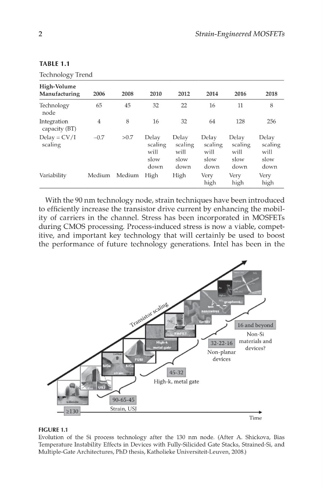
With the 90 nm technology node, strain techniques have been introduced
to efficiently increase the transistor drive current by enhancing the mobility of carriers in the channel. Stress has been incorporated in MOSFETs
during CMOS processing. Process-induced stress is now a viable, competitive, and important key technology that will certainly be used to boost
the performance of future technology generations. Intel has been in the
≥130
90-65-45
Strain, USJ
45-32
High-k, metal gate
T r a n s i s t o r s c a l i n g
32-22-16
Non-planar
devices
16 and beyond
Time
Non-Si
materials and
devices?
FIGURE 1.1
Evolution of the Si process technology after the 130 nm node. (After A. Shickova, Bias
Temperature Instability Effects in Devices with Fully-Silicided Gate Stacks, Strained-Si, and
Multiple-Gate Architectures, PhD thesis, Katholieke Universiteit-Leuven, 2008.)
TABLE 1.1
Technology Trend
High-Volume
Manufacturing
2006
2008
2010
2012
2014
2016
2018
Technology
node
65
45
32
22
16
11
8
Integration
capacity (BT)
4
8
16
32
64
128
256
Delay = CV/I
scaling
∼0.7
>0.7
Delay
scaling
will
slow
down
Delay
scaling
will
slow
down
Delay
scaling
will
slow
down
Delay
scaling
will
slow
down
Delay
scaling
will
slow
down
Variability
Medium Medium High
High
Very
high
Very
high
Very
high
Strain-Engineered MOSFETs
With the 90 nm technology node, strain techniques have been introduced
to efficiently increase the transistor drive current by enhancing the mobility of carriers in the channel. Stress has been incorporated in MOSFETs
during CMOS processing. Process-induced stress is now a viable, competitive, and important key technology that will certainly be used to boost
the performance of future technology generations. Intel has been in the
≥130
90-65-45
Strain, USJ
45-32
High-k, metal gate
T r a n s i s t o r s c a l i n g
32-22-16
Non-planar
devices
16 and beyond
Time
Non-Si
materials and
devices?
FIGURE 1.1
Evolution of the Si process technology after the 130 nm node. (After A. Shickova, Bias
Temperature Instability Effects in Devices with Fully-Silicided Gate Stacks, Strained-Si, and
Multiple-Gate Architectures, PhD thesis, Katholieke Universiteit-Leuven, 2008.)
TABLE 1.1
Technology Trend
High-Volume
Manufacturing
2006
2008
2010
2012
2014
2016
2018
Technology
node
65
45
32
22
16
11
8
Integration
capacity (BT)
4
8
16
32
64
128
256
Delay = CV/I
scaling
∼0.7
>0.7
Delay
scaling
will
slow
down
Delay
scaling
will
slow
down
Delay
scaling
will
slow
down
Delay
scaling
will
slow
down
Delay
scaling
will
slow
down
Variability
Medium Medium High
High
Very
high
Very
high
Very
high