

236
Strain-Engineered MOSFETs
N it generation depends on the curvature (or the interfacial strain at the Si
substrate) and suggests the existence of strain (compressive strain) at the Si/
SiO 2 interface. Strained bonds and bond defects such as Si dangling bond or
Si-H bond in the network of SiO 2 films are responsible for the generation of
hole traps that are mostly distributed near the Si/SiO 2 interface [10]. The compressive strain reduces the interatomic distance on the SiO 2 side more than
that on the Si substrate side at the Si/SiO 2 interface region when the reference
wafer turns from convex to concave. Therefore, the bond mismatch at the
Si/SiO 2 interface becomes very small. Thus, N it generation is less due to the
marked variation of bond mismatch at the Si/SiO 2 interface. N it generation is
also reaction-diffusion (R-D) limited.
The Si dangling bond generated can consequently be traced to be at a new
equilibrium position with a different bond reformation probability. Since
a drastic change of interatomic distance does not occur within the Si/SiO 2
interface due to compressive strain, the bond reformation efficiency is high
and broken bonds are repaired in the region of compressive strain [12]. Thus,
the results indicate that compressive strain does not create favourable conditions for additional interface state creation. Figure 8.1 shows that interface
state generation for drain bias V ds = 50 mV, which depends on temperature,
with N it being higher for devices stressed at a higher temperature.
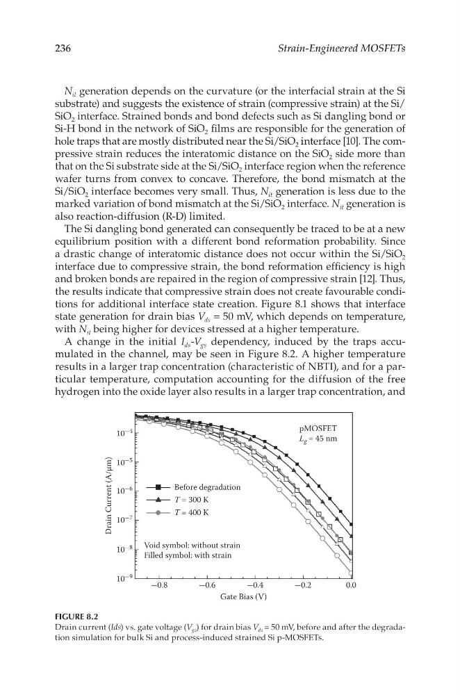
A change in the initial I ds -V gs dependency, induced by the traps accumulated in the channel, may be seen in Figure 8.2. A higher temperature
results in a larger trap concentration (characteristic of NBTI), and for a particular temperature, computation accounting for the diffusion of the free
hydrogen into the oxide layer also results in a larger trap concentration, and
10
4
10
5
10
6
10
7
10
8
10
9
0.8
0.6
0.4
Gate Bias (V)
0.2
0.0
Before degradation
pMOSFET
L g = 45 nm
T = 300 K
T = 400 K
Void symbol: without strain
Filled symbol: with strain
Drain Current (A/μm)
FIGURE 8.2
Drain current (Ids) vs. gate voltage (V gs ) for drain bias V ds = 50 mV, before and after the degradation simulation for bulk Si and process-induced strained Si p-MOSFETs.
Strain-Engineered MOSFETs
N it generation depends on the curvature (or the interfacial strain at the Si
substrate) and suggests the existence of strain (compressive strain) at the Si/
SiO 2 interface. Strained bonds and bond defects such as Si dangling bond or
Si-H bond in the network of SiO 2 films are responsible for the generation of
hole traps that are mostly distributed near the Si/SiO 2 interface [10]. The compressive strain reduces the interatomic distance on the SiO 2 side more than
that on the Si substrate side at the Si/SiO 2 interface region when the reference
wafer turns from convex to concave. Therefore, the bond mismatch at the
Si/SiO 2 interface becomes very small. Thus, N it generation is less due to the
marked variation of bond mismatch at the Si/SiO 2 interface. N it generation is
also reaction-diffusion (R-D) limited.
The Si dangling bond generated can consequently be traced to be at a new
equilibrium position with a different bond reformation probability. Since
a drastic change of interatomic distance does not occur within the Si/SiO 2
interface due to compressive strain, the bond reformation efficiency is high
and broken bonds are repaired in the region of compressive strain [12]. Thus,
the results indicate that compressive strain does not create favourable conditions for additional interface state creation. Figure 8.1 shows that interface
state generation for drain bias V ds = 50 mV, which depends on temperature,
with N it being higher for devices stressed at a higher temperature.
A change in the initial I ds -V gs dependency, induced by the traps accumulated in the channel, may be seen in Figure 8.2. A higher temperature
results in a larger trap concentration (characteristic of NBTI), and for a particular temperature, computation accounting for the diffusion of the free
hydrogen into the oxide layer also results in a larger trap concentration, and
10
4
10
5
10
6
10
7
10
8
10
9
0.8
0.6
0.4
Gate Bias (V)
0.2
0.0
Before degradation
pMOSFET
L g = 45 nm
T = 300 K
T = 400 K
Void symbol: without strain
Filled symbol: with strain
Drain Current (A/μm)
FIGURE 8.2
Drain current (Ids) vs. gate voltage (V gs ) for drain bias V ds = 50 mV, before and after the degradation simulation for bulk Si and process-induced strained Si p-MOSFETs.