

235
Reliability and Degradation of Strain-Engineered MOSFETs
the mobility model, appropriate mobility values were defined in the fields of
the parameter file. Mainly, the NBTI effect is based on interface trap generation due to broken Si-H bonds at the semiconductor/oxide interface, which is
a rough surface where the highly ordered crystalline strained Si channel and
the amorphous SiO 2 dielectric meet. The interface traps generated during
NBTI lead to parametric shifts at the MOSFET level. These interface states
can shift the threshold voltage of the strain-engineered p-MOSFET as
= ε
V t
t
N z t
T
ox
ox
D i
( )
( , )
2
(8.10)
where ε ox is the dielectric constant of the SiO 2 and t ox is the thickness of the oxide.
8.2 Simulation of NBTI in p-MOSFETs
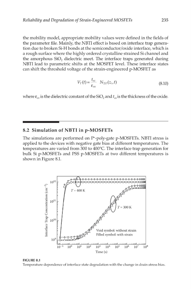
The simulations are performed on P + -poly-gate p-MOSFETs. NBTI stress is
applied to the devices with negative gate bias at different temperatures. The
temperatures are varied from 300 to 400°C. The interface trap generation for
bulk Si p-MOSFETs and PSS p-MOSFETs at two different temperatures is
shown in Figure 8.1.
10
12
10
11
10
10
10
9
10
1 10
0
10
1
10
2
10
3
Time (s)
T = 300 K
T = 400 K
10
4
10
5
10
6
10
7
10
8
Void symbol: without strain
Filled symbol: with strain
Interface Trap Concentration (cm
–2
)
FIGURE 8.1
Temperature dependence of interface state degradation with the change in drain stress bias.
Reliability and Degradation of Strain-Engineered MOSFETs
the mobility model, appropriate mobility values were defined in the fields of
the parameter file. Mainly, the NBTI effect is based on interface trap generation due to broken Si-H bonds at the semiconductor/oxide interface, which is
a rough surface where the highly ordered crystalline strained Si channel and
the amorphous SiO 2 dielectric meet. The interface traps generated during
NBTI lead to parametric shifts at the MOSFET level. These interface states
can shift the threshold voltage of the strain-engineered p-MOSFET as
= ε
V t
t
N z t
T
ox
ox
D i
( )
( , )
2
(8.10)
where ε ox is the dielectric constant of the SiO 2 and t ox is the thickness of the oxide.
8.2 Simulation of NBTI in p-MOSFETs
The simulations are performed on P + -poly-gate p-MOSFETs. NBTI stress is
applied to the devices with negative gate bias at different temperatures. The
temperatures are varied from 300 to 400°C. The interface trap generation for
bulk Si p-MOSFETs and PSS p-MOSFETs at two different temperatures is
shown in Figure 8.1.
10
12
10
11
10
10
10
9
10
1 10
0
10
1
10
2
10
3
Time (s)
T = 300 K
T = 400 K
10
4
10
5
10
6
10
7
10
8
Void symbol: without strain
Filled symbol: with strain
Interface Trap Concentration (cm
–2
)
FIGURE 8.1
Temperature dependence of interface state degradation with the change in drain stress bias.