

237
Reliability and Degradation of Strain-Engineered MOSFETs
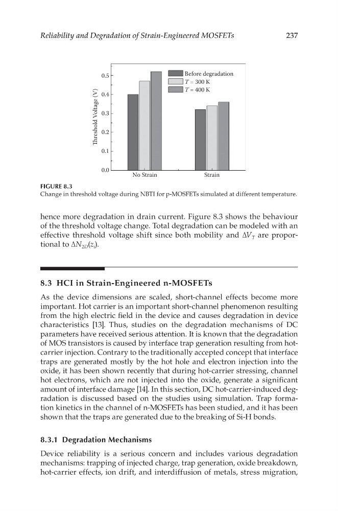
hence more degradation in drain current. Figure 8.3 shows the behaviour
of the threshold voltage change. Total degradation can be modeled with an
effective threshold voltage shift since both mobility and ΔV T are proportional to ΔN 2D (z i ).
8.3 HCI in Strain-Engineered n-MOSFETs
As the device dimensions are scaled, short-channel effects become more
important. Hot carrier is an important short-channel phenomenon resulting
from the high electric field in the device and causes degradation in device
characteristics [13]. Thus, studies on the degradation mechanisms of DC
parameters have received serious attention. It is known that the degradation
of MOS transistors is caused by interface trap generation resulting from hotcarrier injection. Contrary to the traditionally accepted concept that interface
traps are generated mostly by the hot hole and electron injection into the
oxide, it has been shown recently that during hot-carrier stressing, channel
hot electrons, which are not injected into the oxide, generate a significant
amount of interface damage [14]. In this section, DC hot-carrier-induced degradation is discussed based on the studies using simulation. Trap formation kinetics in the channel of n-MOSFETs has been studied, and it has been
shown that the traps are generated due to the breaking of Si-H bonds.
8.3.1 Degradation Mechanisms
Device reliability is a serious concern and includes various degradation
mechanisms: trapping of injected charge, trap generation, oxide breakdown,
hot-carrier effects, ion drift, and interdiffusion of metals, stress migration,
FIGURE 8.3
Change in threshold voltage during NBTI for p-MOSFETs simulated at different temperature.
Reliability and Degradation of Strain-Engineered MOSFETs
hence more degradation in drain current. Figure 8.3 shows the behaviour
of the threshold voltage change. Total degradation can be modeled with an
effective threshold voltage shift since both mobility and ΔV T are proportional to ΔN 2D (z i ).
8.3 HCI in Strain-Engineered n-MOSFETs
As the device dimensions are scaled, short-channel effects become more
important. Hot carrier is an important short-channel phenomenon resulting
from the high electric field in the device and causes degradation in device
characteristics [13]. Thus, studies on the degradation mechanisms of DC
parameters have received serious attention. It is known that the degradation
of MOS transistors is caused by interface trap generation resulting from hotcarrier injection. Contrary to the traditionally accepted concept that interface
traps are generated mostly by the hot hole and electron injection into the
oxide, it has been shown recently that during hot-carrier stressing, channel
hot electrons, which are not injected into the oxide, generate a significant
amount of interface damage [14]. In this section, DC hot-carrier-induced degradation is discussed based on the studies using simulation. Trap formation kinetics in the channel of n-MOSFETs has been studied, and it has been
shown that the traps are generated due to the breaking of Si-H bonds.
8.3.1 Degradation Mechanisms
Device reliability is a serious concern and includes various degradation
mechanisms: trapping of injected charge, trap generation, oxide breakdown,
hot-carrier effects, ion drift, and interdiffusion of metals, stress migration,
FIGURE 8.3
Change in threshold voltage during NBTI for p-MOSFETs simulated at different temperature.