

232
Strain-Engineered MOSFETs
are prone to higher NBTI. In strained Si MOSFETs, due to crystal lattice mismatch at the Si/SiO 2 interface, traps are present in the form of a Si dangling
bond. During fabrication, MOSFETs are annealed in hydrogen ambient to
passivate the dangling Si bonds. Also, strain present at the Si/SiO 2 interface
degrades the reliability by weakening the H 2 -passivated Si dangling (Si-H)
bonds by creating favourable conditions for interface state generation [8, 9].
The traps increase the threshold voltage, reduce the channel mobility due
to higher scattering, induce parasitic capacitances in transistors, and lead to
drain current degradation in the course of time.
In this section, we use Synopsys technology computer-aided design
(TCAD) tools for simulation of trap generation at the Si/SiO 2 interface of
p-MOSFETs with e-SiGe (SiGe pocket in the source and drain region) under
negative gate bias. We account for the passivity of silicon dangling bonds by
free hydrogen and its diffusion in the bulk oxide region and the activation
energy of the Si-H bond process, which depends on the hydrogen concentration. The trap concentrations as a function of time in the bulk Si and processinduced strained Si p-MOSFET are compared. An analytical trap-induced
Coulomb mobility model is developed and implemented in the SDevice simulator. We discuss in detail the influence of NBTI on the DC characteristics
of strain-engineered p-MOSFETs.
8.1.1 Quasi-2D Coulomb Mobility Model
The strained Si/SiO 2 interface in strain-engineered p-MOSFETs shows a very
large number of trap states [9]. These traps become filled during inversion,
causing a change of conduction charge in the inversion layer and an increase in
the Coulomb scattering of mobile charges. Owing to the large number of occupied interface traps, Coulomb interaction is likely to be an important scattering mechanism in process-induced strained Si p-MOSFET operation. Coulomb
interaction results in very low surface mobilities and may be described by a
quasi-2D scattering model. The Coulomb potential due to the occupied traps
and fixed charges decreases with distance away from the interface. Mobile
charges in the inversion layer that are close to the interface are scattered more
than those farther away from the interface; therefore, the Coulomb scattering
mobility model is required to be depth dependent. We assume that the electron gas can move in the x-y plane and is confined in the z direction. Electrons
are considered confined or quantised if their deBroglie wavelength is larger
than or comparable to the width of the confining potential. The deBroglie
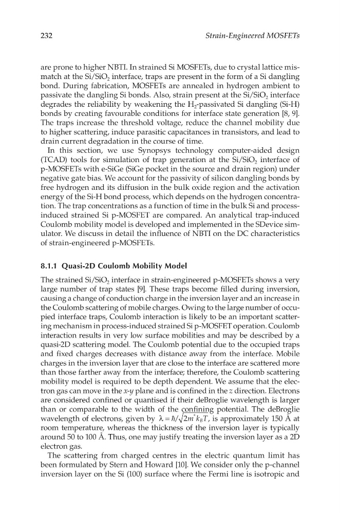
wavelength of electrons, given by
λ =
m k T
B
/ 2
*
, is approximately 150 Å at
room temperature, whereas the thickness of the inversion layer is typically
around 50 to 100 Å. Thus, one may justify treating the inversion layer as a 2D
electron gas.
The scattering from charged centres in the electric quantum limit has
been formulated by Stern and Howard [10]. We consider only the p-channel
inversion layer on the Si (100) surface where the Fermi line is isotropic and
Strain-Engineered MOSFETs
are prone to higher NBTI. In strained Si MOSFETs, due to crystal lattice mismatch at the Si/SiO 2 interface, traps are present in the form of a Si dangling
bond. During fabrication, MOSFETs are annealed in hydrogen ambient to
passivate the dangling Si bonds. Also, strain present at the Si/SiO 2 interface
degrades the reliability by weakening the H 2 -passivated Si dangling (Si-H)
bonds by creating favourable conditions for interface state generation [8, 9].
The traps increase the threshold voltage, reduce the channel mobility due
to higher scattering, induce parasitic capacitances in transistors, and lead to
drain current degradation in the course of time.
In this section, we use Synopsys technology computer-aided design
(TCAD) tools for simulation of trap generation at the Si/SiO 2 interface of
p-MOSFETs with e-SiGe (SiGe pocket in the source and drain region) under
negative gate bias. We account for the passivity of silicon dangling bonds by
free hydrogen and its diffusion in the bulk oxide region and the activation
energy of the Si-H bond process, which depends on the hydrogen concentration. The trap concentrations as a function of time in the bulk Si and processinduced strained Si p-MOSFET are compared. An analytical trap-induced
Coulomb mobility model is developed and implemented in the SDevice simulator. We discuss in detail the influence of NBTI on the DC characteristics
of strain-engineered p-MOSFETs.
8.1.1 Quasi-2D Coulomb Mobility Model
The strained Si/SiO 2 interface in strain-engineered p-MOSFETs shows a very
large number of trap states [9]. These traps become filled during inversion,
causing a change of conduction charge in the inversion layer and an increase in
the Coulomb scattering of mobile charges. Owing to the large number of occupied interface traps, Coulomb interaction is likely to be an important scattering mechanism in process-induced strained Si p-MOSFET operation. Coulomb
interaction results in very low surface mobilities and may be described by a
quasi-2D scattering model. The Coulomb potential due to the occupied traps
and fixed charges decreases with distance away from the interface. Mobile
charges in the inversion layer that are close to the interface are scattered more
than those farther away from the interface; therefore, the Coulomb scattering
mobility model is required to be depth dependent. We assume that the electron gas can move in the x-y plane and is confined in the z direction. Electrons
are considered confined or quantised if their deBroglie wavelength is larger
than or comparable to the width of the confining potential. The deBroglie
wavelength of electrons, given by
λ =
m k T
B
/ 2
*
, is approximately 150 Å at
room temperature, whereas the thickness of the inversion layer is typically
around 50 to 100 Å. Thus, one may justify treating the inversion layer as a 2D
electron gas.
The scattering from charged centres in the electric quantum limit has
been formulated by Stern and Howard [10]. We consider only the p-channel
inversion layer on the Si (100) surface where the Fermi line is isotropic and