

233
Reliability and Degradation of Strain-Engineered MOSFETs
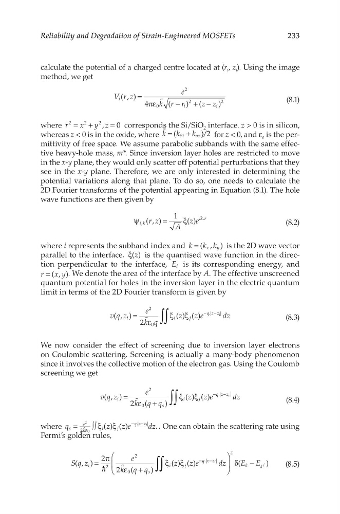
calculate the potential of a charged centre located at (r i , z i ). Using the image
method, we get
= πε
−
+ −
V r z
e
k r r
z z
i
i
i
( , )
4
(
) (
)
2
0
2
2
(8.1)
where r
x y z
,
0
2
2
2
= +
= corresponds the Si/SiO 2 interface. z > 0 is in silicon,
whereas z < 0 is in the oxide, where
(
) /2
k k
k
Si
ox
=
+
for z < 0, and ε o is the permittivity of free space. We assume parabolic subbands with the same effective heavy-hole mass, m*. Since inversion layer holes are restricted to move
in the x-y plane, they would only scatter off potential perturbations that they
see in the x-y plane. Therefore, we are only interested in determining the
potential variations along that plane. To do so, one needs to calculate the
2D Fourier transforms of the potential appearing in Equation (8.1). The hole
wave functions are then given by
ψ
=
ξ
r z
A
z e
i k
ik r
( , )
1 ( )
,
.
(8.2)
where i represents the subband index and =
k k k
x
y
( , ) is the 2D wave vector
parallel to the interface. ξ z
( ) is the quantised wave function in the direction perpendicular to the interface, E i is its corresponding energy, and
=
r x y
( , ). We denote the area of the interface by A. The effective unscreened
quantum potential for holes in the inversion layer in the electric quantum
limit in terms of the 2D Fourier transform is given by
∫∫
= ε
ξ ξ
−
−
v q z
e
k q
z
z e
dz
i
i
j
q z zi
( , ) 2
( ) ( )
2
0
. | |
(8.3)
We now consider the effect of screening due to inversion layer electrons
on Coulombic scattering. Screening is actually a many-body phenomenon
since it involves the collective motion of the electron gas. Using the Coulomb
screening we get
∫∫
= ε +
ξ ξ
−
−
v q z
e
k q q
z
z e
dz
i
s
i
j
q z zi
( , ) 2 (
)
( ) ( )
2
0
. |
|
(8.4)
where q
z
z e
dz
s
e
k
i
j
q z zi
( ) ( )
.
2
.
| |
2
0
=
∫∫ ξ ξ
ε
− −
. One can obtain the scattering rate using
Fermi’s golden rules,
∫∫
=
π
ε +
ξ ξ
δ
−
−
−
S q z
e
k q q
z
z e
dz
E E
i
s
i
j
q z z
k
k
i
( , )
2
2 (
)
( ) ( )
(
)
2
2
0
. |
|
2
/
(8.5)
Reliability and Degradation of Strain-Engineered MOSFETs
calculate the potential of a charged centre located at (r i , z i ). Using the image
method, we get
= πε
−
+ −
V r z
e
k r r
z z
i
i
i
( , )
4
(
) (
)
2
0
2
2
(8.1)
where r
x y z
,
0
2
2
2
= +
= corresponds the Si/SiO 2 interface. z > 0 is in silicon,
whereas z < 0 is in the oxide, where
(
) /2
k k
k
Si
ox
=
+
for z < 0, and ε o is the permittivity of free space. We assume parabolic subbands with the same effective heavy-hole mass, m*. Since inversion layer holes are restricted to move
in the x-y plane, they would only scatter off potential perturbations that they
see in the x-y plane. Therefore, we are only interested in determining the
potential variations along that plane. To do so, one needs to calculate the
2D Fourier transforms of the potential appearing in Equation (8.1). The hole
wave functions are then given by
ψ
=
ξ
r z
A
z e
i k
ik r
( , )
1 ( )
,
.
(8.2)
where i represents the subband index and =
k k k
x
y
( , ) is the 2D wave vector
parallel to the interface. ξ z
( ) is the quantised wave function in the direction perpendicular to the interface, E i is its corresponding energy, and
=
r x y
( , ). We denote the area of the interface by A. The effective unscreened
quantum potential for holes in the inversion layer in the electric quantum
limit in terms of the 2D Fourier transform is given by
∫∫
= ε
ξ ξ
−
−
v q z
e
k q
z
z e
dz
i
i
j
q z zi
( , ) 2
( ) ( )
2
0
. | |
(8.3)
We now consider the effect of screening due to inversion layer electrons
on Coulombic scattering. Screening is actually a many-body phenomenon
since it involves the collective motion of the electron gas. Using the Coulomb
screening we get
∫∫
= ε +
ξ ξ
−
−
v q z
e
k q q
z
z e
dz
i
s
i
j
q z zi
( , ) 2 (
)
( ) ( )
2
0
. |
|
(8.4)
where q
z
z e
dz
s
e
k
i
j
q z zi
( ) ( )
.
2
.
| |
2
0
=
∫∫ ξ ξ
ε
− −
. One can obtain the scattering rate using
Fermi’s golden rules,
∫∫
=
π
ε +
ξ ξ
δ
−
−
−
S q z
e
k q q
z
z e
dz
E E
i
s
i
j
q z z
k
k
i
( , )
2
2 (
)
( ) ( )
(
)
2
2
0
. |
|
2
/
(8.5)