

225
Technology CAD of Strain-Engineered MOSFETs
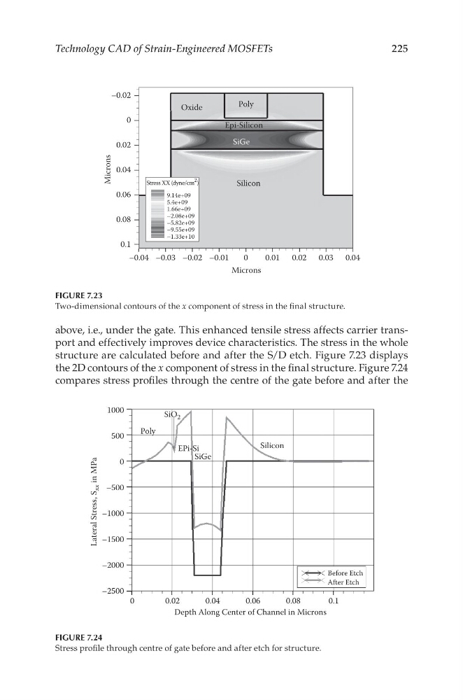
above, i.e., under the gate. This enhanced tensile stress affects carrier transport and effectively improves device characteristics. The stress in the whole
structure are calculated before and after the S/D etch. Figure 7.23 displays
the 2D contours of the x component of stress in the final structure. Figure 7.24
compares stress profiles through the centre of the gate before and after the
Microns
–0.02
0
0.02
0.04
0.06
0.08
0.1
–0.04 –0.03 –0.02 –0.01
Silicon
SiGe
Poly
Oxide
Epi-Silicon
Stress XX (dyne/cm
2
)
9.14e+09
5.4e+09
1.66e+09
–2.08e+09
–5.82e+09
–9.55e+09
–1.33e+10
0
Microns
0.01 0.02 0.03 0.04
FIGURE 7.23
Two-dimensional contours of the x component of stress in the final structure.
1000
500
–500
–1000
Lateral Stress, S
xx in MPa
–1500
–2000
–2500
0
0.02
0.04
0.06
Depth Along Center of Channel in Microns
0.08
0.1
Before Etch
After Etch
0
Poly
EPi-Si
SiGe
Silicon
SiO 2
FIGURE 7.24
Stress profile through centre of gate before and after etch for structure.
Technology CAD of Strain-Engineered MOSFETs
above, i.e., under the gate. This enhanced tensile stress affects carrier transport and effectively improves device characteristics. The stress in the whole
structure are calculated before and after the S/D etch. Figure 7.23 displays
the 2D contours of the x component of stress in the final structure. Figure 7.24
compares stress profiles through the centre of the gate before and after the
Microns
–0.02
0
0.02
0.04
0.06
0.08
0.1
–0.04 –0.03 –0.02 –0.01
Silicon
SiGe
Poly
Oxide
Epi-Silicon
Stress XX (dyne/cm
2
)
9.14e+09
5.4e+09
1.66e+09
–2.08e+09
–5.82e+09
–9.55e+09
–1.33e+10
0
Microns
0.01 0.02 0.03 0.04
FIGURE 7.23
Two-dimensional contours of the x component of stress in the final structure.
1000
500
–500
–1000
Lateral Stress, S
xx in MPa
–1500
–2000
–2500
0
0.02
0.04
0.06
Depth Along Center of Channel in Microns
0.08
0.1
Before Etch
After Etch
0
Poly
EPi-Si
SiGe
Silicon
SiO 2
FIGURE 7.24
Stress profile through centre of gate before and after etch for structure.