

223
Technology CAD of Strain-Engineered MOSFETs
high-speed strain-engineered CMOS device design. Since f T depends on
both the C gs and g m , it is important to clarify the impact. The improvements
observed in devices are driven primarily by stress-induced enhancement of
g m as C gs is almost identical for devices with different stress and orientation
configurations.
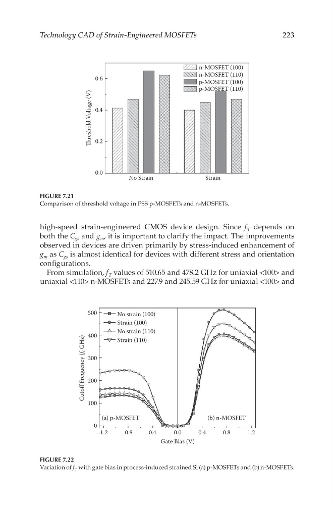
From simulation, f T values of 510.65 and 478.2 GHz for uniaxial <100> and
uniaxial <110> n-MOSFETs and 227.9 and 245.59 GHz for uniaxial <100> and
0.6
0.4
0.2
reshold Voltage (V)
0.0
No Strain
Strain
n-MOSFET (100)
n-MOSFET (110)
p-MOSFET (110)
p-MOSFET (100)
FIGURE 7.21
Comparison of threshold voltage in PSS p-MOSFETs and n-MOSFETs.
No strain (100)
No strain (110)
Strain (100)
Strain (110)
400
500
300
200
Cutoff Frequency (f
t GHz)
100
–1.2
–0.8
–0.4
0.0
Gate Bias (V)
0.4
0.8
1.2
0
(a) p-MOSFET
(b) n-MOSFET
FIGURE 7.22
Variation of f T with gate bias in process-induced strained Si (a) p-MOSFETs and (b) n-MOSFETs.
Technology CAD of Strain-Engineered MOSFETs
high-speed strain-engineered CMOS device design. Since f T depends on
both the C gs and g m , it is important to clarify the impact. The improvements
observed in devices are driven primarily by stress-induced enhancement of
g m as C gs is almost identical for devices with different stress and orientation
configurations.
From simulation, f T values of 510.65 and 478.2 GHz for uniaxial <100> and
uniaxial <110> n-MOSFETs and 227.9 and 245.59 GHz for uniaxial <100> and
0.6
0.4
0.2
reshold Voltage (V)
0.0
No Strain
Strain
n-MOSFET (100)
n-MOSFET (110)
p-MOSFET (110)
p-MOSFET (100)
FIGURE 7.21
Comparison of threshold voltage in PSS p-MOSFETs and n-MOSFETs.
No strain (100)
No strain (110)
Strain (100)
Strain (110)
400
500
300
200
Cutoff Frequency (f
t GHz)
100
–1.2
–0.8
–0.4
0.0
Gate Bias (V)
0.4
0.8
1.2
0
(a) p-MOSFET
(b) n-MOSFET
FIGURE 7.22
Variation of f T with gate bias in process-induced strained Si (a) p-MOSFETs and (b) n-MOSFETs.