

222
Strain-Engineered MOSFETs
The variation of f T with V gs for PSS p- and n-MOSFET is shown in
Figure 7.22(a) and (b), respectively. It is found that the f T is higher in the <110>
direction than in the <100> direction with stress for PSS p-MOSFETs. For PSS
n-MOSFETs, f T is higher in the <100> direction than the <110> direction with
stress and without stress. These results indicate the advantages of straindependent mobility enhancement along with hybrid orientation toward a
2000
100
110
With strain
No strain
No strain
V ds = 1.25 V
V gs = 1.25 V
(a) p-MOSFET
(b) n-MOSFET
With strain
1600
1200
Drain Current (µA/µm)
800
400
0
–1.2
–0.8
–0.4
Drain Bias (V)
0.0
0.4
0.8
1.2
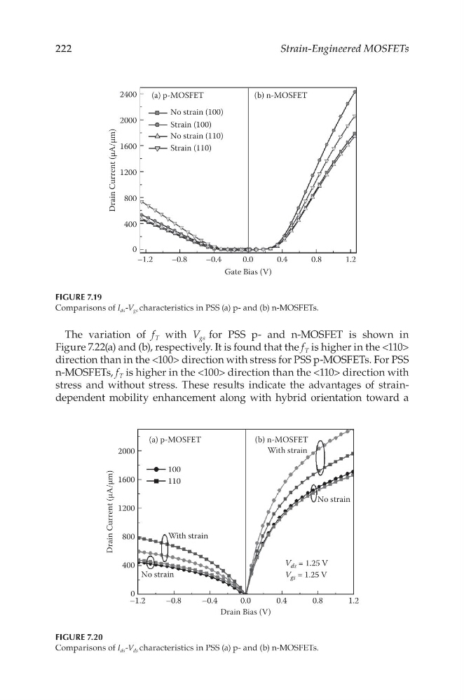
FIGURE 7.20
Comparisons of I ds -V ds characteristics in PSS (a) p- and (b) n-MOSFETs.
2400
2000
1600
1200
Drain Current (µA/µm)
800
400
0
–1.2
–0.8
–0.4
0.0
Gate Bias (V)
0.4
0.8
1.2
No strain (100)
No strain (110)
Strain (100)
Strain (110)
(a) p-MOSFET
(b) n-MOSFET
FIGURE 7.19
Comparisons of I ds -V gs characteristics in PSS (a) p- and (b) n-MOSFETs.
Strain-Engineered MOSFETs
The variation of f T with V gs for PSS p- and n-MOSFET is shown in
Figure 7.22(a) and (b), respectively. It is found that the f T is higher in the <110>
direction than in the <100> direction with stress for PSS p-MOSFETs. For PSS
n-MOSFETs, f T is higher in the <100> direction than the <110> direction with
stress and without stress. These results indicate the advantages of straindependent mobility enhancement along with hybrid orientation toward a
2000
100
110
With strain
No strain
No strain
V ds = 1.25 V
V gs = 1.25 V
(a) p-MOSFET
(b) n-MOSFET
With strain
1600
1200
Drain Current (µA/µm)
800
400
0
–1.2
–0.8
–0.4
Drain Bias (V)
0.0
0.4
0.8
1.2
FIGURE 7.20
Comparisons of I ds -V ds characteristics in PSS (a) p- and (b) n-MOSFETs.
2400
2000
1600
1200
Drain Current (µA/µm)
800
400
0
–1.2
–0.8
–0.4
0.0
Gate Bias (V)
0.4
0.8
1.2
No strain (100)
No strain (110)
Strain (100)
Strain (110)
(a) p-MOSFET
(b) n-MOSFET
FIGURE 7.19
Comparisons of I ds -V gs characteristics in PSS (a) p- and (b) n-MOSFETs.