

221
Technology CAD of Strain-Engineered MOSFETs
and drain regions are idealised by a short box doped to 1 × 10 20 cm –3 and
present negligible series resistance. The value of the gate resistance (R gate )
is added via postprocessing to the TCAD simulations. Process-induced
strained p-MOSFET with 45 nm gate length was simulated for different surface orientation. Figure 7.19(a) compares the drain current against the gate
voltage characteristics for the devices with compressive stress. The corresponding 2D device simulation shows a slightly higher drive current due to
stress. An improvement in drive current in the <110> direction is observed
over the drive current in the <100> direction under the longitudinal uniaxial
compressive stress and is of much significance. For comparison, 45 nm gate
length process-induced strained channel n-MOSFETs with different surface
orientations were also simulated. Figure 7.19(b) compares the drain current
against the gate voltage characteristics for the devices with a highly tensile
cap layer and a relaxed capping layer. The corresponding 2D simulation
shows a higher current (of the order of 14–15%) gain due to stress. Figure 7.20
compares the drain current against the drain voltage characteristics. In case
of n-MOSFETs, devices with a highly tensile cap layer show a slightly higher
current gain due to stress (~15%) than the device with a relaxed capping layer.
It also shows a drive current improvement in the <100> direction, more
than in the <110> under the longitudinal uniaxial tensile stress, and it is of
much significance to HOT. Also, p-MOSFETs with compressive stress show
higher drain current than bulk Si MOSFETs. A higher drive current in the
<110> direction than in the <100> direction is observed under the longitudinal uniaxial compressive stress. Figure 7.21 shows a comparison of threshold
voltage for both the HOT MOSFETs and PSS MOSFETs.
500
400
300
f
T (GHz)
200
100
0
–1.2
–0.8
–0.4
0.0
Gate Voltage (V)
0.4
0.8
1.2
Without strain
Process-induced strain
(a) pMOSFET
(b) nMOSFET
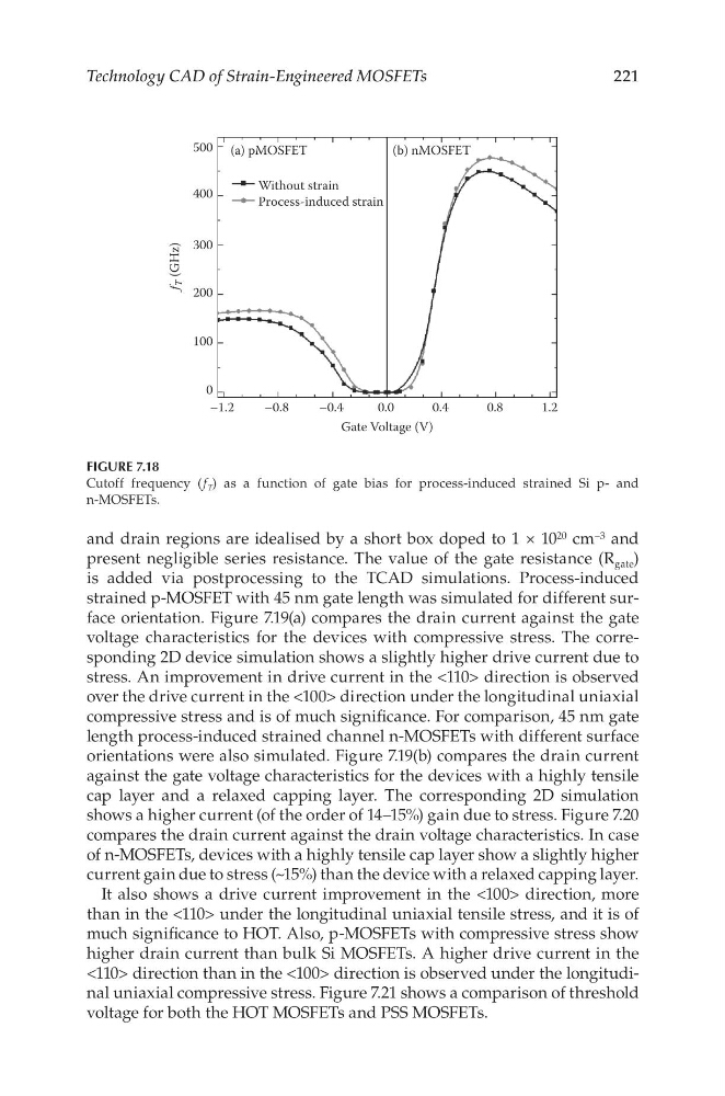
FIGURE 7.18
Cutoff frequency (f T ) as a function of gate bias for process-induced strained Si p- and
n-MOSFETs.
Technology CAD of Strain-Engineered MOSFETs
and drain regions are idealised by a short box doped to 1 × 10 20 cm –3 and
present negligible series resistance. The value of the gate resistance (R gate )
is added via postprocessing to the TCAD simulations. Process-induced
strained p-MOSFET with 45 nm gate length was simulated for different surface orientation. Figure 7.19(a) compares the drain current against the gate
voltage characteristics for the devices with compressive stress. The corresponding 2D device simulation shows a slightly higher drive current due to
stress. An improvement in drive current in the <110> direction is observed
over the drive current in the <100> direction under the longitudinal uniaxial
compressive stress and is of much significance. For comparison, 45 nm gate
length process-induced strained channel n-MOSFETs with different surface
orientations were also simulated. Figure 7.19(b) compares the drain current
against the gate voltage characteristics for the devices with a highly tensile
cap layer and a relaxed capping layer. The corresponding 2D simulation
shows a higher current (of the order of 14–15%) gain due to stress. Figure 7.20
compares the drain current against the drain voltage characteristics. In case
of n-MOSFETs, devices with a highly tensile cap layer show a slightly higher
current gain due to stress (~15%) than the device with a relaxed capping layer.
It also shows a drive current improvement in the <100> direction, more
than in the <110> under the longitudinal uniaxial tensile stress, and it is of
much significance to HOT. Also, p-MOSFETs with compressive stress show
higher drain current than bulk Si MOSFETs. A higher drive current in the
<110> direction than in the <100> direction is observed under the longitudinal uniaxial compressive stress. Figure 7.21 shows a comparison of threshold
voltage for both the HOT MOSFETs and PSS MOSFETs.
500
400
300
f
T (GHz)
200
100
0
–1.2
–0.8
–0.4
0.0
Gate Voltage (V)
0.4
0.8
1.2
Without strain
Process-induced strain
(a) pMOSFET
(b) nMOSFET
FIGURE 7.18
Cutoff frequency (f T ) as a function of gate bias for process-induced strained Si p- and
n-MOSFETs.