

220
Strain-Engineered MOSFETs
7.4 AC Performance
Since scaled p- and n-MOSFETs may find applications in the RF regime, it is
necessary to develop some figures of merit to assess the device performance.
Using SDevice transient simulation, based on the mobility models described
before, small-signal analysis has been performed to extract RF parameters
for process-induced strained Si MOSFETs.
An AC simulation is performed at equidistant bias points for small-signal AC
analysis at various frequencies, with the gate as the input port, the drain as the
output port, and the source and substrate grounded. The resulting small-signal
admittance and capacitance parameters are then used to extract a RF figure of
merit, such as the cutoff frequency (f T ). The bias dependence of f T is shown in
Figure 7.18. We extracted f T using the following expression, in which the current gain, |h 21 |, is converted from the s parameters using the transformation:
h
s
s
s
s s
(1
)(1
)
21
21
11
22
12 21
=
−
−
+
+
(7.4)
7.5 Hybrid Orientation Technology for
Strain-Engineered MOSFETs
In this section, we present the technology computer-aided design (TCAD)
and simulation results for both the stress engineered n- and p-MOSFETs
on <100> and <110> hybrid orientation substrates, respectively. The source
100
99
98
97
SS (mV/decade)
96
0.39
0.42
0.45
Nitride Film Stress (GPa)
0.48
0.51
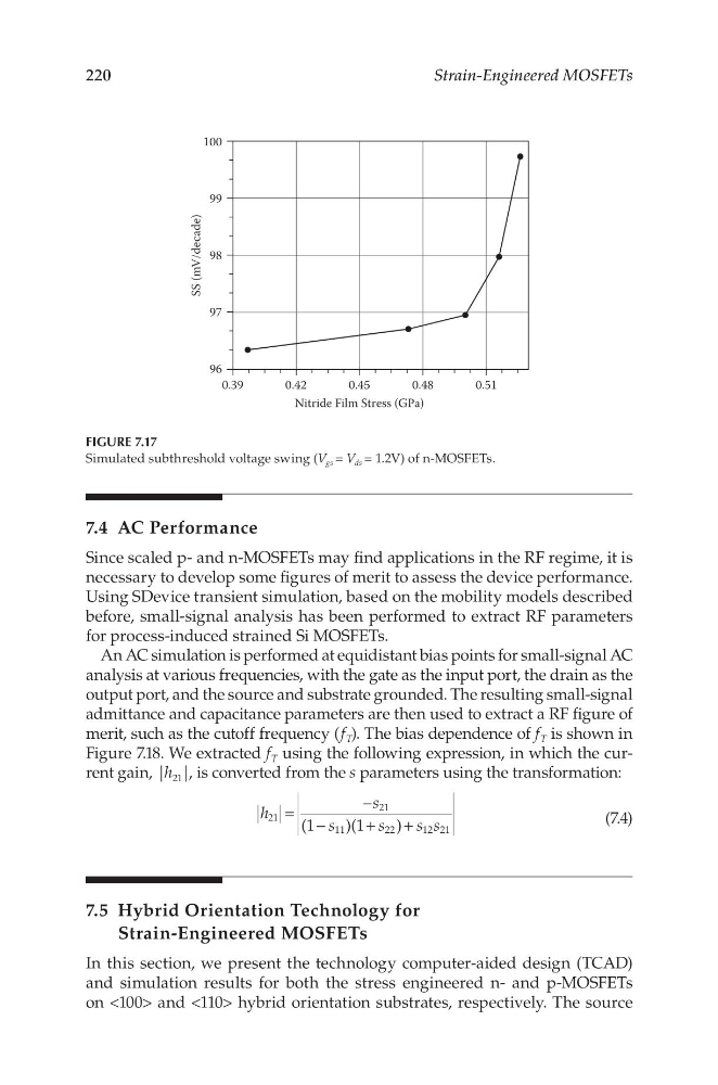
FIGURE 7.17
Simulated subthreshold voltage swing (V gs = V ds = 1.2V) of n-MOSFETs.
Strain-Engineered MOSFETs
7.4 AC Performance
Since scaled p- and n-MOSFETs may find applications in the RF regime, it is
necessary to develop some figures of merit to assess the device performance.
Using SDevice transient simulation, based on the mobility models described
before, small-signal analysis has been performed to extract RF parameters
for process-induced strained Si MOSFETs.
An AC simulation is performed at equidistant bias points for small-signal AC
analysis at various frequencies, with the gate as the input port, the drain as the
output port, and the source and substrate grounded. The resulting small-signal
admittance and capacitance parameters are then used to extract a RF figure of
merit, such as the cutoff frequency (f T ). The bias dependence of f T is shown in
Figure 7.18. We extracted f T using the following expression, in which the current gain, |h 21 |, is converted from the s parameters using the transformation:
h
s
s
s
s s
(1
)(1
)
21
21
11
22
12 21
=
−
−
+
+
(7.4)
7.5 Hybrid Orientation Technology for
Strain-Engineered MOSFETs
In this section, we present the technology computer-aided design (TCAD)
and simulation results for both the stress engineered n- and p-MOSFETs
on <100> and <110> hybrid orientation substrates, respectively. The source
100
99
98
97
SS (mV/decade)
96
0.39
0.42
0.45
Nitride Film Stress (GPa)
0.48
0.51
FIGURE 7.17
Simulated subthreshold voltage swing (V gs = V ds = 1.2V) of n-MOSFETs.