

219
Technology CAD of Strain-Engineered MOSFETs
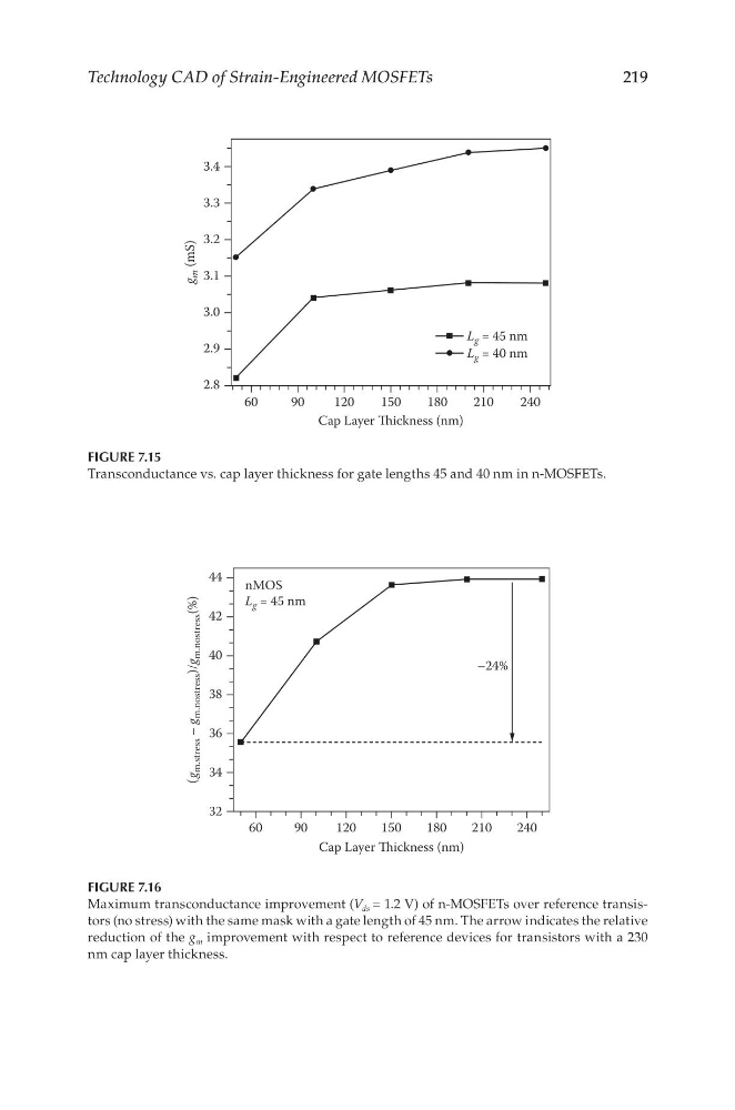
FIGURE 7.15
Transconductance vs. cap layer thickness for gate lengths 45 and 40 nm in n-MOSFETs.
60
90
120
150
180
210
240
32
34
36
38
40
42
44
–24%
nMOS
L g = 45 nm
(g
m.stress – g
m.nostress )/g
m.nostress (%)
Cap Layer ickness (nm)
FIGURE 7.16
Maximum transconductance improvement (V ds = 1.2 V) of n-MOSFETs over reference transistors (no stress) with the same mask with a gate length of 45 nm. The arrow indicates the relative
reduction of the g m improvement with respect to reference devices for transistors with a 230
nm cap layer thickness.
Technology CAD of Strain-Engineered MOSFETs
FIGURE 7.15
Transconductance vs. cap layer thickness for gate lengths 45 and 40 nm in n-MOSFETs.
60
90
120
150
180
210
240
32
34
36
38
40
42
44
–24%
nMOS
L g = 45 nm
(g
m.stress – g
m.nostress )/g
m.nostress (%)
Cap Layer ickness (nm)
FIGURE 7.16
Maximum transconductance improvement (V ds = 1.2 V) of n-MOSFETs over reference transistors (no stress) with the same mask with a gate length of 45 nm. The arrow indicates the relative
reduction of the g m improvement with respect to reference devices for transistors with a 230
nm cap layer thickness.