

218
Strain-Engineered MOSFETs
0.2
0.4
0.6
0.8
1.0
1.2
1.4
Channel Stress ε xx (GPa)
117.0
116.5
116.0
115.5
SS (mV/decade)
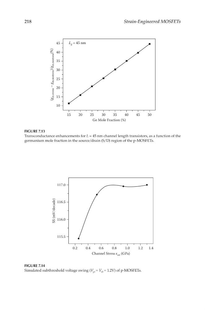
FIGURE 7.14
Simulated subthreshold voltage swing (V gs = V ds = 1.2V) of p-MOSFETs.
45
40
35
30
25
20
15
10
15
20
25
30
35
Ge Mole Fraction (%)
40
45
50
L g = 45 nm
(g
m.stress – g
m.nostress )/g
m.nostress (%)
FIGURE 7.13
Transconductance enhancements for L = 45 nm channel length transistors, as a function of the
germanium mole fraction in the source/drain (S/D) region of the p-MOSFETs.
Strain-Engineered MOSFETs
0.2
0.4
0.6
0.8
1.0
1.2
1.4
Channel Stress ε xx (GPa)
117.0
116.5
116.0
115.5
SS (mV/decade)
FIGURE 7.14
Simulated subthreshold voltage swing (V gs = V ds = 1.2V) of p-MOSFETs.
45
40
35
30
25
20
15
10
15
20
25
30
35
Ge Mole Fraction (%)
40
45
50
L g = 45 nm
(g
m.stress – g
m.nostress )/g
m.nostress (%)
FIGURE 7.13
Transconductance enhancements for L = 45 nm channel length transistors, as a function of the
germanium mole fraction in the source/drain (S/D) region of the p-MOSFETs.