

217
Technology CAD of Strain-Engineered MOSFETs
enhancement is approximately the same as the linear drain current enhancement. Using Equation (7.3), we have computed the electron and hole mobility
enhancement factor due to tensile and compressive longitudinal stress for
strain-engineered n- or p-MOSFETs, respectively. For the PSS p- and n-MOSFETs, hole and electron mobility enhancement factors have been found to
be ~1.5× and ~1.8× that of bulk Si, which is also consistent with our simulation results. The resulting simulation demonstrates an approximately 17%
enhancement of drain current with respect to the conventional silicon p-MOSFET. The impact of a strained Si channel on device performance is evaluated
in Sentaurus Device by enhancing the mobility by an amount consistent with
that which can be realised in practise with embedded SiGe S/D layers for
p-MOSFETs and a highly tensile silicon-nitride cap layer for n-MOSFETs.
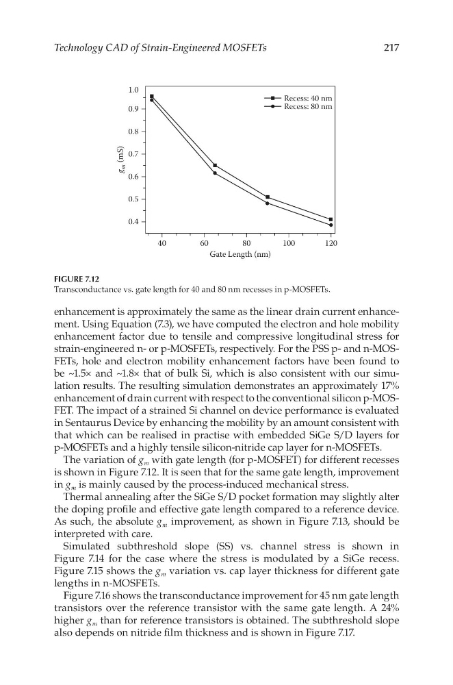
The variation of g m with gate length (for p-MOSFET) for different recesses
is shown in Figure 7.12. It is seen that for the same gate length, improvement
in g m is mainly caused by the process-induced mechanical stress.
Thermal annealing after the SiGe S/D pocket formation may slightly alter
the doping profile and effective gate length compared to a reference device.
As such, the absolute g m improvement, as shown in Figure 7.13, should be
interpreted with care.
Simulated subthreshold slope (SS) vs. channel stress is shown in
Figure 7.14 for the case where the stress is modulated by a SiGe recess.
Figure 7.15 shows the g m variation vs. cap layer thickness for different gate
lengths in n-MOSFETs.
Figure 7.16 shows the transconductance improvement for 45 nm gate length
transistors over the reference transistor with the same gate length. A 24%
higher g m than for reference transistors is obtained. The subthreshold slope
also depends on nitride film thickness and is shown in Figure 7.17.
Recess: 40 nm
Recess: 80 nm
40
60
80
Gate Length (nm)
100
120
1.0
0.9
0.8
0.7
g
m (mS)
0.6
0.5
0.4
FIGURE 7.12
Transconductance vs. gate length for 40 and 80 nm recesses in p-MOSFETs.
Technology CAD of Strain-Engineered MOSFETs
enhancement is approximately the same as the linear drain current enhancement. Using Equation (7.3), we have computed the electron and hole mobility
enhancement factor due to tensile and compressive longitudinal stress for
strain-engineered n- or p-MOSFETs, respectively. For the PSS p- and n-MOSFETs, hole and electron mobility enhancement factors have been found to
be ~1.5× and ~1.8× that of bulk Si, which is also consistent with our simulation results. The resulting simulation demonstrates an approximately 17%
enhancement of drain current with respect to the conventional silicon p-MOSFET. The impact of a strained Si channel on device performance is evaluated
in Sentaurus Device by enhancing the mobility by an amount consistent with
that which can be realised in practise with embedded SiGe S/D layers for
p-MOSFETs and a highly tensile silicon-nitride cap layer for n-MOSFETs.
The variation of g m with gate length (for p-MOSFET) for different recesses
is shown in Figure 7.12. It is seen that for the same gate length, improvement
in g m is mainly caused by the process-induced mechanical stress.
Thermal annealing after the SiGe S/D pocket formation may slightly alter
the doping profile and effective gate length compared to a reference device.
As such, the absolute g m improvement, as shown in Figure 7.13, should be
interpreted with care.
Simulated subthreshold slope (SS) vs. channel stress is shown in
Figure 7.14 for the case where the stress is modulated by a SiGe recess.
Figure 7.15 shows the g m variation vs. cap layer thickness for different gate
lengths in n-MOSFETs.
Figure 7.16 shows the transconductance improvement for 45 nm gate length
transistors over the reference transistor with the same gate length. A 24%
higher g m than for reference transistors is obtained. The subthreshold slope
also depends on nitride film thickness and is shown in Figure 7.17.
Recess: 40 nm
Recess: 80 nm
40
60
80
Gate Length (nm)
100
120
1.0
0.9
0.8
0.7
g
m (mS)
0.6
0.5
0.4
FIGURE 7.12
Transconductance vs. gate length for 40 and 80 nm recesses in p-MOSFETs.