

216
Strain-Engineered MOSFETs
linear drain current has been reported in [6]. The change in linear drain current for p-MOSFETs may be expressed as [7]
I
I
I
I
I
a
a
a
dlinStSi
dlinSi
dlinSi
dlin
dlin
x xx
y yy
z zz
−
=
= ε + ε + ε
(7.3)
where a x , a y , and a z are the strain sensitivity coefficients with respect to the x,
y, and z strain components, respectively. Since ΔI dlin /I dlin ≈ Δµ/µ, the mobility
2.4
2.0
(a) pMOSFET
Without strain
Process induced strain
(b) nMOSFET
1.6
1.2
Drain Current (mA/μm)
0.8
0.4
0.0
–1.2
–0.8
V gs = 1.2 V
V gs = 1.0 V
V gs = 0.8 V
V gs = 0.6 V
V gs = 0.05 V
V gs = 0.6 V
V gs = 0.8 V
V gs = 1.0 V
–0.4
0.0
Drain Bias (V)
0.4
0.8
1.2
V gs = 1.2 V
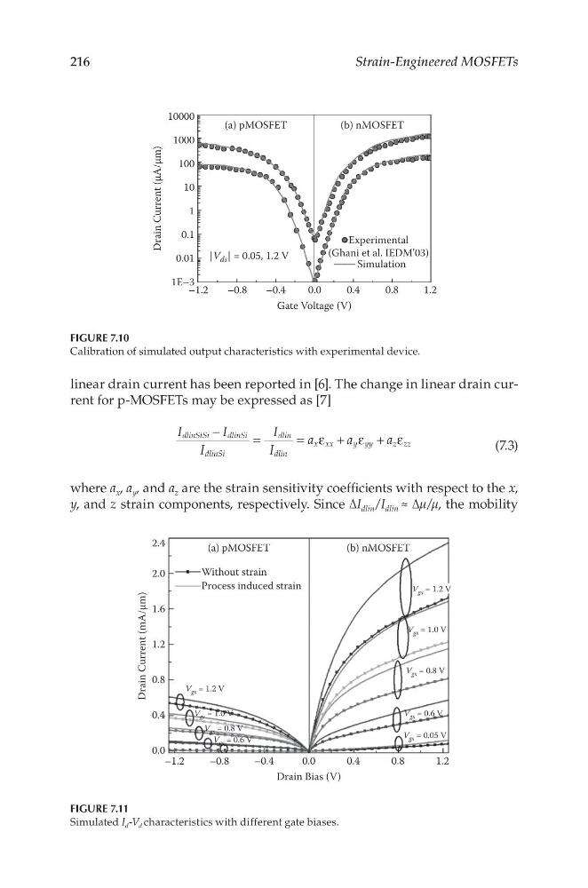
FIGURE 7.11
Simulated I d -V d characteristics with different gate biases.
10000
1000
100
10
1
0.1
0.01
1E–3
–1.2
–0.8
–0.4
0.0
Gate Voltage (V)
Experimental
(Ghani et al. IEDM’03)
Simulation
|V ds | = 0.05, 1.2 V
0.4
0.8
1.2
Drain Current (μA/μm)
(a) pMOSFET
( b) nMOSFET
FIGURE 7.10
Calibration of simulated output characteristics with experimental device.
Strain-Engineered MOSFETs
linear drain current has been reported in [6]. The change in linear drain current for p-MOSFETs may be expressed as [7]
I
I
I
I
I
a
a
a
dlinStSi
dlinSi
dlinSi
dlin
dlin
x xx
y yy
z zz
−
=
= ε + ε + ε
(7.3)
where a x , a y , and a z are the strain sensitivity coefficients with respect to the x,
y, and z strain components, respectively. Since ΔI dlin /I dlin ≈ Δµ/µ, the mobility
2.4
2.0
(a) pMOSFET
Without strain
Process induced strain
(b) nMOSFET
1.6
1.2
Drain Current (mA/μm)
0.8
0.4
0.0
–1.2
–0.8
V gs = 1.2 V
V gs = 1.0 V
V gs = 0.8 V
V gs = 0.6 V
V gs = 0.05 V
V gs = 0.6 V
V gs = 0.8 V
V gs = 1.0 V
–0.4
0.0
Drain Bias (V)
0.4
0.8
1.2
V gs = 1.2 V
FIGURE 7.11
Simulated I d -V d characteristics with different gate biases.
10000
1000
100
10
1
0.1
0.01
1E–3
–1.2
–0.8
–0.4
0.0
Gate Voltage (V)
Experimental
(Ghani et al. IEDM’03)
Simulation
|V ds | = 0.05, 1.2 V
0.4
0.8
1.2
Drain Current (μA/μm)
(a) pMOSFET
( b) nMOSFET
FIGURE 7.10
Calibration of simulated output characteristics with experimental device.