

215
Technology CAD of Strain-Engineered MOSFETs
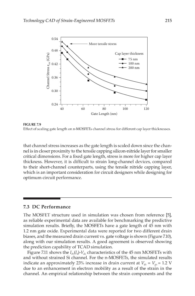
that channel stress increases as the gate length is scaled down since the channel is in closer proximity to the tensile capping silicon-nitride layer for smaller
critical dimensions. For a fixed gate length, stress is more for higher cap layer
thickness. However, it is difficult to strain long-channel devices, compared
to their short-channel counterparts, using the tensile nitride capping layer,
which is an important consideration for circuit designers while designing for
optimum circuit performance.
7.3 DC Performance
The MOSFET structure used in simulation was chosen from reference [5],
as reliable experimental data are available for benchmarking the predictive
simulation results. Briefly, the MOSFETs have a gate length of 45 nm with
1.2 nm gate oxide. Experimental data were reported for two different drain
biases, and the measured drain current vs. gate voltage is shown (Figure 7.10),
along with our simulation results. A good agreement is observed showing
the prediction capability of TCAD simulation.
Figure 7.11 shows the I ds (I d )-V ds characteristics of the 45 nm MOSFETs with
and without strained Si channel. For the n-MOSFETs, the simulated results
indicate an approximately 23% increase in drain current at V ds = V gs = 1.2 V
due to an enhancement in electron mobility as a result of the strain in the
channel. An empirical relationship between the strain components and the
0.54
0.48
More tensile stress
Cap layer thickness
75 nm
100 nm
200 nm
0.42
0.36
0.30
0.24
40
60
80
Gate Length (nm)
100
120
Channel Stress ε
xx (GPa)
FIGURE 7.9
Effect of scaling gate length on n-MOSFETs channel stress for different cap layer thicknesses.
Technology CAD of Strain-Engineered MOSFETs
that channel stress increases as the gate length is scaled down since the channel is in closer proximity to the tensile capping silicon-nitride layer for smaller
critical dimensions. For a fixed gate length, stress is more for higher cap layer
thickness. However, it is difficult to strain long-channel devices, compared
to their short-channel counterparts, using the tensile nitride capping layer,
which is an important consideration for circuit designers while designing for
optimum circuit performance.
7.3 DC Performance
The MOSFET structure used in simulation was chosen from reference [5],
as reliable experimental data are available for benchmarking the predictive
simulation results. Briefly, the MOSFETs have a gate length of 45 nm with
1.2 nm gate oxide. Experimental data were reported for two different drain
biases, and the measured drain current vs. gate voltage is shown (Figure 7.10),
along with our simulation results. A good agreement is observed showing
the prediction capability of TCAD simulation.
Figure 7.11 shows the I ds (I d )-V ds characteristics of the 45 nm MOSFETs with
and without strained Si channel. For the n-MOSFETs, the simulated results
indicate an approximately 23% increase in drain current at V ds = V gs = 1.2 V
due to an enhancement in electron mobility as a result of the strain in the
channel. An empirical relationship between the strain components and the
0.54
0.48
More tensile stress
Cap layer thickness
75 nm
100 nm
200 nm
0.42
0.36
0.30
0.24
40
60
80
Gate Length (nm)
100
120
Channel Stress ε
xx (GPa)
FIGURE 7.9
Effect of scaling gate length on n-MOSFETs channel stress for different cap layer thicknesses.