

211
Technology CAD of Strain-Engineered MOSFETs
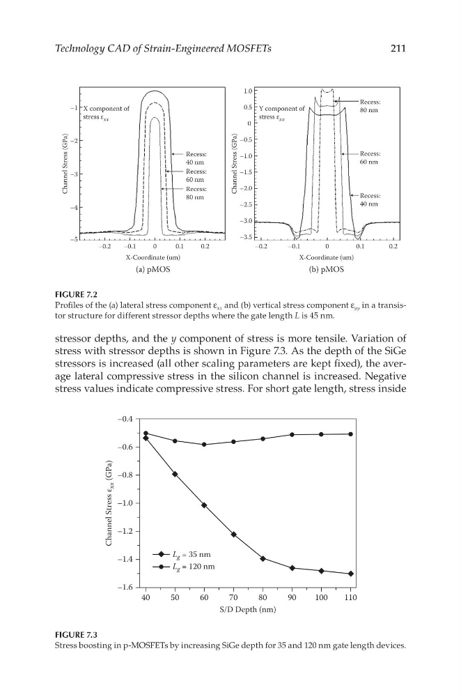
stressor depths, and the y component of stress is more tensile. Variation of
stress with stressor depths is shown in Figure 7.3. As the depth of the SiGe
stressors is increased (all other scaling parameters are kept fixed), the average lateral compressive stress in the silicon channel is increased. Negative
stress values indicate compressive stress. For short gate length, stress inside
X component of
stress ε xx
Y component of
stress ε xx
–1
–2
–3
–4
–5
–0.2
–0.1
0
X-Coordinate (um)
(a) pMOS
0.1
Recess:
40 nm
1.0
0.5
0
–0.5
–1.0
–1.5
–2.0
–2.5
–3.0
–3.5
Recess:
60 nm
Recess:
80 nm
0.2
–0.2
–0.1
0
X-Coordinate (um)
(b) pMOS
0.1
0.2
Channel Stress (GPa)
Channel Stress (GPa)
Recess:
80 nm
Recess:
60 nm
Recess:
40 nm
FIGURE 7.2
Profiles of the (a) lateral stress component ε xx and (b) vertical stress component ε yy in a transistor structure for different stressor depths where the gate length L is 45 nm.
–0.4
–0.6
–0.8
–1.0
Channel Stress ε
xx (GPa)
–1.2
–1.4
–1.6
40
50
60
70
80
S/D Depth (nm)
L g = 35 nm
L g = 120 nm
90
100
110
FIGURE 7.3
Stress boosting in p-MOSFETs by increasing SiGe depth for 35 and 120 nm gate length devices.
Technology CAD of Strain-Engineered MOSFETs
stressor depths, and the y component of stress is more tensile. Variation of
stress with stressor depths is shown in Figure 7.3. As the depth of the SiGe
stressors is increased (all other scaling parameters are kept fixed), the average lateral compressive stress in the silicon channel is increased. Negative
stress values indicate compressive stress. For short gate length, stress inside
X component of
stress ε xx
Y component of
stress ε xx
–1
–2
–3
–4
–5
–0.2
–0.1
0
X-Coordinate (um)
(a) pMOS
0.1
Recess:
40 nm
1.0
0.5
0
–0.5
–1.0
–1.5
–2.0
–2.5
–3.0
–3.5
Recess:
60 nm
Recess:
80 nm
0.2
–0.2
–0.1
0
X-Coordinate (um)
(b) pMOS
0.1
0.2
Channel Stress (GPa)
Channel Stress (GPa)
Recess:
80 nm
Recess:
60 nm
Recess:
40 nm
FIGURE 7.2
Profiles of the (a) lateral stress component ε xx and (b) vertical stress component ε yy in a transistor structure for different stressor depths where the gate length L is 45 nm.
–0.4
–0.6
–0.8
–1.0
Channel Stress ε
xx (GPa)
–1.2
–1.4
–1.6
40
50
60
70
80
S/D Depth (nm)
L g = 35 nm
L g = 120 nm
90
100
110
FIGURE 7.3
Stress boosting in p-MOSFETs by increasing SiGe depth for 35 and 120 nm gate length devices.