

210
Strain-Engineered MOSFETs
shows the stress distribution of the 3D device structure obtained from
SProcess simulation.
The structure generated by SProcess is then simulated using SDevice [4].
The simulated device performance includes DC electrostatic behaviour with
strain-induced mobility enhancement and the impact of rapid thermal
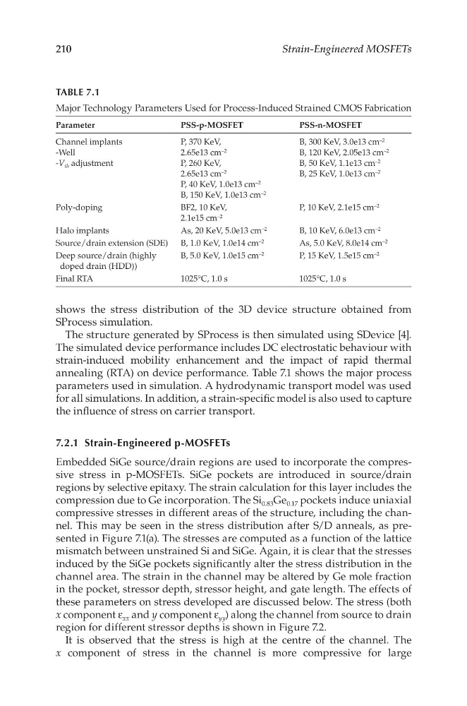
annealing (RTA) on device performance. Table 7.1 shows the major process
parameters used in simulation. A hydrodynamic transport model was used
for all simulations. In addition, a strain-specific model is also used to capture
the influence of stress on carrier transport.
7.2.1 Strain-Engineered p-MOSFETs
Embedded SiGe source/drain regions are used to incorporate the compressive stress in p-MOSFETs. SiGe pockets are introduced in source/drain
regions by selective epitaxy. The strain calculation for this layer includes the
compression due to Ge incorporation. The Si 0.83 Ge 0.17 pockets induce uniaxial
compressive stresses in different areas of the structure, including the channel. This may be seen in the stress distribution after S/D anneals, as presented in Figure 7.1(a). The stresses are computed as a function of the lattice
mismatch between unstrained Si and SiGe. Again, it is clear that the stresses
induced by the SiGe pockets significantly alter the stress distribution in the
channel area. The strain in the channel may be altered by Ge mole fraction
in the pocket, stressor depth, stressor height, and gate length. The effects of
these parameters on stress developed are discussed below. The stress (both
x component ε xx and y component ε yy ) along the channel from source to drain
region for different stressor depths is shown in Figure 7.2.
It is observed that the stress is high at the centre of the channel. The
x component of stress in the channel is more compressive for large
TABLE 7.1
Major Technology Parameters Used for Process-Induced Strained CMOS Fabrication
Parameter
PSS-p-MOSFET
PSS-n-MOSFET
Channel implants
-Well
-V th adjustment
P, 370 KeV,
2.65e13 cm –2
P, 260 KeV,
2.65e13 cm –2
P, 40 KeV, 1.0e13 cm –2
B, 150 KeV, 1.0e13 cm –2
B, 300 KeV, 3.0e13 cm –2
B, 120 KeV, 2.05e13 cm –2
B, 50 KeV, 1.1e13 cm –2
B, 25 KeV, 1.0e13 cm –2
Poly-doping
BF2, 10 KeV,
2.1e15 cm –2
P, 10 KeV, 2.1e15 cm –2
Halo implants
As, 20 KeV, 5.0e13 cm –2
B, 10 KeV, 6.0e13 cm –2
Source/drain extension (SDE) B, 1.0 KeV, 1.0e14 cm –2
As, 5.0 KeV, 8.0e14 cm –2
Deep source/drain (highly
doped drain (HDD))
B, 5.0 KeV, 1.0e15 cm –2
P, 15 KeV, 1.5e15 cm –2
Final RTA
1025°C, 1.0 s
1025°C, 1.0 s
Strain-Engineered MOSFETs
shows the stress distribution of the 3D device structure obtained from
SProcess simulation.
The structure generated by SProcess is then simulated using SDevice [4].
The simulated device performance includes DC electrostatic behaviour with
strain-induced mobility enhancement and the impact of rapid thermal
annealing (RTA) on device performance. Table 7.1 shows the major process
parameters used in simulation. A hydrodynamic transport model was used
for all simulations. In addition, a strain-specific model is also used to capture
the influence of stress on carrier transport.
7.2.1 Strain-Engineered p-MOSFETs
Embedded SiGe source/drain regions are used to incorporate the compressive stress in p-MOSFETs. SiGe pockets are introduced in source/drain
regions by selective epitaxy. The strain calculation for this layer includes the
compression due to Ge incorporation. The Si 0.83 Ge 0.17 pockets induce uniaxial
compressive stresses in different areas of the structure, including the channel. This may be seen in the stress distribution after S/D anneals, as presented in Figure 7.1(a). The stresses are computed as a function of the lattice
mismatch between unstrained Si and SiGe. Again, it is clear that the stresses
induced by the SiGe pockets significantly alter the stress distribution in the
channel area. The strain in the channel may be altered by Ge mole fraction
in the pocket, stressor depth, stressor height, and gate length. The effects of
these parameters on stress developed are discussed below. The stress (both
x component ε xx and y component ε yy ) along the channel from source to drain
region for different stressor depths is shown in Figure 7.2.
It is observed that the stress is high at the centre of the channel. The
x component of stress in the channel is more compressive for large
TABLE 7.1
Major Technology Parameters Used for Process-Induced Strained CMOS Fabrication
Parameter
PSS-p-MOSFET
PSS-n-MOSFET
Channel implants
-Well
-V th adjustment
P, 370 KeV,
2.65e13 cm –2
P, 260 KeV,
2.65e13 cm –2
P, 40 KeV, 1.0e13 cm –2
B, 150 KeV, 1.0e13 cm –2
B, 300 KeV, 3.0e13 cm –2
B, 120 KeV, 2.05e13 cm –2
B, 50 KeV, 1.1e13 cm –2
B, 25 KeV, 1.0e13 cm –2
Poly-doping
BF2, 10 KeV,
2.1e15 cm –2
P, 10 KeV, 2.1e15 cm –2
Halo implants
As, 20 KeV, 5.0e13 cm –2
B, 10 KeV, 6.0e13 cm –2
Source/drain extension (SDE) B, 1.0 KeV, 1.0e14 cm –2
As, 5.0 KeV, 8.0e14 cm –2
Deep source/drain (highly
doped drain (HDD))
B, 5.0 KeV, 1.0e15 cm –2
P, 15 KeV, 1.5e15 cm –2
Final RTA
1025°C, 1.0 s
1025°C, 1.0 s