

209
Technology CAD of Strain-Engineered MOSFETs
A three-stream diffusion model is used. Additionally, formation of point
defect clusters and the three-phase segregation model accounting for the
dose loss at the silicon/oxide interface are considered. For simulation of ion
implantation, a 2D analytic integration with dual-Pearson (in silicon) and
Pearson distribution functions (in other materials) is used. In process simulation, the Hobler model is used to simulate the damage profiles and amorphisation. For the simulation of Ge diffusion and redistribution in strained
Si a model is developed that supports structures with various regions containing strained Si. The effect of change in material composition due to Ge
diffusion and its effect on strain (for p-MOSFETs) are also incorporated. At
each diffusion step, the stress evolution is computed, including oxidation
steps based on the viscoelastic model. This model is also used to compute
the stress effects on n-MOSFETs after the deposition of the highly tensile
cap layer. Although successful demonstrations of both n- and p-type experimental strained Si MOSFETs have been made, little information is available
on the performance of scaled strained Si MOSFETs with gate length less
than 50 nm. Note that the strained Si layer thickness is kept unchanged
since simulations show that variation of the strained Si layer thickness from
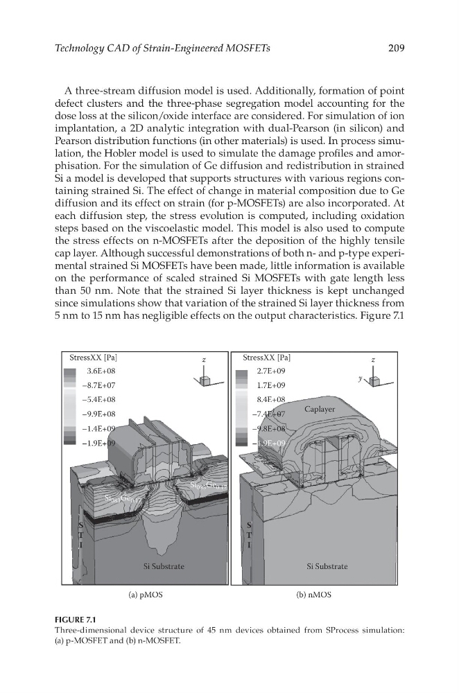
5 nm to 15 nm has negligible effects on the output characteristics. Figure 7.1
StressXX [Pa]
3.6E+08
–8.7E+07
(a) pMOS
z
–5.4E+08
–9.9E+08
–1.4E+09
–1.9E+09
StressXX [Pa]
2.7E+09
1.7E+09
(b) nMOS
z
y
8.4E+08
–7.4E+07
–9.8E+08
Caplayer
–1.9E+09
Si Substrate
S
T
I
S
T
I
Si Substrate
Si 083 Ge 0.17
Si 083 Ge 0.17
FIGURE 7.1
Three-dimensional device structure of 45 nm devices obtained from SProcess simulation:
(a) p-MOSFET and (b) n-MOSFET.
Technology CAD of Strain-Engineered MOSFETs
A three-stream diffusion model is used. Additionally, formation of point
defect clusters and the three-phase segregation model accounting for the
dose loss at the silicon/oxide interface are considered. For simulation of ion
implantation, a 2D analytic integration with dual-Pearson (in silicon) and
Pearson distribution functions (in other materials) is used. In process simulation, the Hobler model is used to simulate the damage profiles and amorphisation. For the simulation of Ge diffusion and redistribution in strained
Si a model is developed that supports structures with various regions containing strained Si. The effect of change in material composition due to Ge
diffusion and its effect on strain (for p-MOSFETs) are also incorporated. At
each diffusion step, the stress evolution is computed, including oxidation
steps based on the viscoelastic model. This model is also used to compute
the stress effects on n-MOSFETs after the deposition of the highly tensile
cap layer. Although successful demonstrations of both n- and p-type experimental strained Si MOSFETs have been made, little information is available
on the performance of scaled strained Si MOSFETs with gate length less
than 50 nm. Note that the strained Si layer thickness is kept unchanged
since simulations show that variation of the strained Si layer thickness from
5 nm to 15 nm has negligible effects on the output characteristics. Figure 7.1
StressXX [Pa]
3.6E+08
–8.7E+07
(a) pMOS
z
–5.4E+08
–9.9E+08
–1.4E+09
–1.9E+09
StressXX [Pa]
2.7E+09
1.7E+09
(b) nMOS
z
y
8.4E+08
–7.4E+07
–9.8E+08
Caplayer
–1.9E+09
Si Substrate
S
T
I
S
T
I
Si Substrate
Si 083 Ge 0.17
Si 083 Ge 0.17
FIGURE 7.1
Three-dimensional device structure of 45 nm devices obtained from SProcess simulation:
(a) p-MOSFET and (b) n-MOSFET.