

208
Strain-Engineered MOSFETs
trends of strained Si/SiGe MOSFETs for radio frequency (RF) applications.
We also propose to combine the advantages of the hybrid orientation technology (HOT) and process-induced local strain (PSS) engineering to improve
CMOS device performance via mobility engineering. Mobility models are
developed and used in predictive simulation. The work is based on simulation, using the commercial TCAD tools from Synopsys. Based on the calibration of the models used, performance predictions of scaled strained Si
MOSFETs are made.
7.2 Simulation of Strain-Engineered MOSFETs
In the following, process-induced stress simulations are performed using
the SProcess simulator with the help of a set of strain models for both the
n- and p-MOSFETs. The basic equations used to compute the strain and
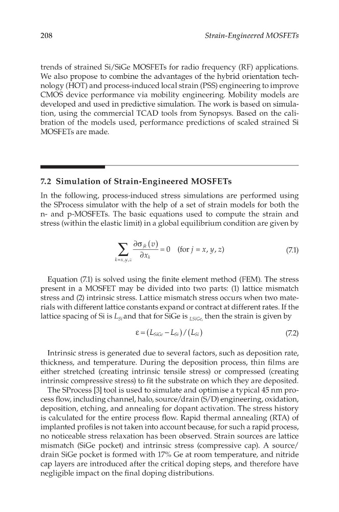
stress (within the elastic limit) in a global equilibrium condition are given by
v
x
j x y z
0 (for = , , )
jk
k
k x y z
, ,
∑
( )
∂σ
∂
=
=
(7.1)
Equation (7.1) is solved using the finite element method (FEM). The stress
present in a MOSFET may be divided into two parts: (1) lattice mismatch
stress and (2) intrinsic stress. Lattice mismatch stress occurs when two materials with different lattice constants expand or contract at different rates. If the
lattice spacing of Si is L Si and that for SiGe is LSiGe, then the strain is given by
L
L
L
/
SiGe
Si
Si
(
) ( )
ε =
−
(7.2)
Intrinsic stress is generated due to several factors, such as deposition rate,
thickness, and temperature. During the deposition process, thin films are
either stretched (creating intrinsic tensile stress) or compressed (creating
intrinsic compressive stress) to fit the substrate on which they are deposited.
The SProcess [3] tool is used to simulate and optimise a typical 45 nm process flow, including channel, halo, source/drain (S/D) engineering, oxidation,
deposition, etching, and annealing for dopant activation. The stress history
is calculated for the entire process flow. Rapid thermal annealing (RTA) of
implanted profiles is not taken into account because, for such a rapid process,
no noticeable stress relaxation has been observed. Strain sources are lattice
mismatch (SiGe pocket) and intrinsic stress (compressive cap). A source/
drain SiGe pocket is formed with 17% Ge at room temperature, and nitride
cap layers are introduced after the critical doping steps, and therefore have
negligible impact on the final doping distributions.
Strain-Engineered MOSFETs
trends of strained Si/SiGe MOSFETs for radio frequency (RF) applications.
We also propose to combine the advantages of the hybrid orientation technology (HOT) and process-induced local strain (PSS) engineering to improve
CMOS device performance via mobility engineering. Mobility models are
developed and used in predictive simulation. The work is based on simulation, using the commercial TCAD tools from Synopsys. Based on the calibration of the models used, performance predictions of scaled strained Si
MOSFETs are made.
7.2 Simulation of Strain-Engineered MOSFETs
In the following, process-induced stress simulations are performed using
the SProcess simulator with the help of a set of strain models for both the
n- and p-MOSFETs. The basic equations used to compute the strain and
stress (within the elastic limit) in a global equilibrium condition are given by
v
x
j x y z
0 (for = , , )
jk
k
k x y z
, ,
∑
( )
∂σ
∂
=
=
(7.1)
Equation (7.1) is solved using the finite element method (FEM). The stress
present in a MOSFET may be divided into two parts: (1) lattice mismatch
stress and (2) intrinsic stress. Lattice mismatch stress occurs when two materials with different lattice constants expand or contract at different rates. If the
lattice spacing of Si is L Si and that for SiGe is LSiGe, then the strain is given by
L
L
L
/
SiGe
Si
Si
(
) ( )
ε =
−
(7.2)
Intrinsic stress is generated due to several factors, such as deposition rate,
thickness, and temperature. During the deposition process, thin films are
either stretched (creating intrinsic tensile stress) or compressed (creating
intrinsic compressive stress) to fit the substrate on which they are deposited.
The SProcess [3] tool is used to simulate and optimise a typical 45 nm process flow, including channel, halo, source/drain (S/D) engineering, oxidation,
deposition, etching, and annealing for dopant activation. The stress history
is calculated for the entire process flow. Rapid thermal annealing (RTA) of
implanted profiles is not taken into account because, for such a rapid process,
no noticeable stress relaxation has been observed. Strain sources are lattice
mismatch (SiGe pocket) and intrinsic stress (compressive cap). A source/
drain SiGe pocket is formed with 17% Ge at room temperature, and nitride
cap layers are introduced after the critical doping steps, and therefore have
negligible impact on the final doping distributions.