

199
Noise in Strain-Engineered Devices
for capture and emission of an electron, τ e and τ c , respectively, are given by
Shockley–Read–Hall statistics, as described by Equation (6.37):
nv
N v
1
,
exp
c
TH n
e
E E
kT
C TH n
(
)
T
F
τ =
σ
τ =
σ
−
where n is electron density in the vicinity of traps and depends on the location of trap in the space charge region and the bias voltage V BE , v TH is the thermal velocity of electrons, σ n is the electron capture cross section of the traps,
N C is the density of state in the conduction band, and E T and E F are the trap
energy level and Fermi potential, respectively.
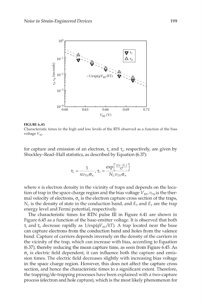
The characteristic times for RTN pulse III in Figure 6.41 are shown in
Figure 6.45 as a function of the base-emitter voltage. It is observed that both
τ l and τ h decrease rapidly as 1/exp(qV BE /kT). A trap located near the base
can capture electrons from the conduction band and holes from the valence
band. Capture of carriers depends inversely on the density of the carriers in
the vicinity of the trap, which can increase with bias, according to Equation
(6.37), thereby reducing the mean capture time, as seen from Figure 6.45. As
σ n is electric field dependent, it can influence both the capture and emission times. The electric field decreases slightly with increasing bias voltage
in the space charge region. However, this does not affect the capture cross
section, and hence the characteristic times to a significant extent. Therefore,
the trapping/de-trapping processes have been explained with a two-capture
process (electron and hole capture), which is the most likely phenomenon for
0.60
10
–4
10
–3
τ
l , τ
h (seconds)
τ l
10
–2
10
–1
10
0
0.63
0.66
V BE (V)
~1/exp(qV BE /kT)
0.69
0.72
τ h
FIGURE 6.45
Characteristic times in the high and low levels of the RTS observed as a function of the bias
voltage V BE .
Noise in Strain-Engineered Devices
for capture and emission of an electron, τ e and τ c , respectively, are given by
Shockley–Read–Hall statistics, as described by Equation (6.37):
nv
N v
1
,
exp
c
TH n
e
E E
kT
C TH n
(
)
T
F
τ =
σ
τ =
σ
−
where n is electron density in the vicinity of traps and depends on the location of trap in the space charge region and the bias voltage V BE , v TH is the thermal velocity of electrons, σ n is the electron capture cross section of the traps,
N C is the density of state in the conduction band, and E T and E F are the trap
energy level and Fermi potential, respectively.
The characteristic times for RTN pulse III in Figure 6.41 are shown in
Figure 6.45 as a function of the base-emitter voltage. It is observed that both
τ l and τ h decrease rapidly as 1/exp(qV BE /kT). A trap located near the base
can capture electrons from the conduction band and holes from the valence
band. Capture of carriers depends inversely on the density of the carriers in
the vicinity of the trap, which can increase with bias, according to Equation
(6.37), thereby reducing the mean capture time, as seen from Figure 6.45. As
σ n is electric field dependent, it can influence both the capture and emission times. The electric field decreases slightly with increasing bias voltage
in the space charge region. However, this does not affect the capture cross
section, and hence the characteristic times to a significant extent. Therefore,
the trapping/de-trapping processes have been explained with a two-capture
process (electron and hole capture), which is the most likely phenomenon for
0.60
10
–4
10
–3
τ
l , τ
h (seconds)
τ l
10
–2
10
–1
10
0
0.63
0.66
V BE (V)
~1/exp(qV BE /kT)
0.69
0.72
τ h
FIGURE 6.45
Characteristic times in the high and low levels of the RTS observed as a function of the bias
voltage V BE .