

200
Strain-Engineered MOSFETs
explaining the strong reduction in characteristic times with V BE , as observed
in Figure 6.45. It may be possible that a more complex capture process is
involved. With the base region containing carbon as recombination centres,
the base doping is usually very high in SiGe:C HBTs, allowing a very thin
width of the base-emitter space charge layer. This thin space charge region
assists tunneling of electrons across it from the neutral regions into the traps
in the spacer oxide. The tunneling thickness reduces with the potential barrier as V BE increases, which reflects the rapid reduction in characteristic times
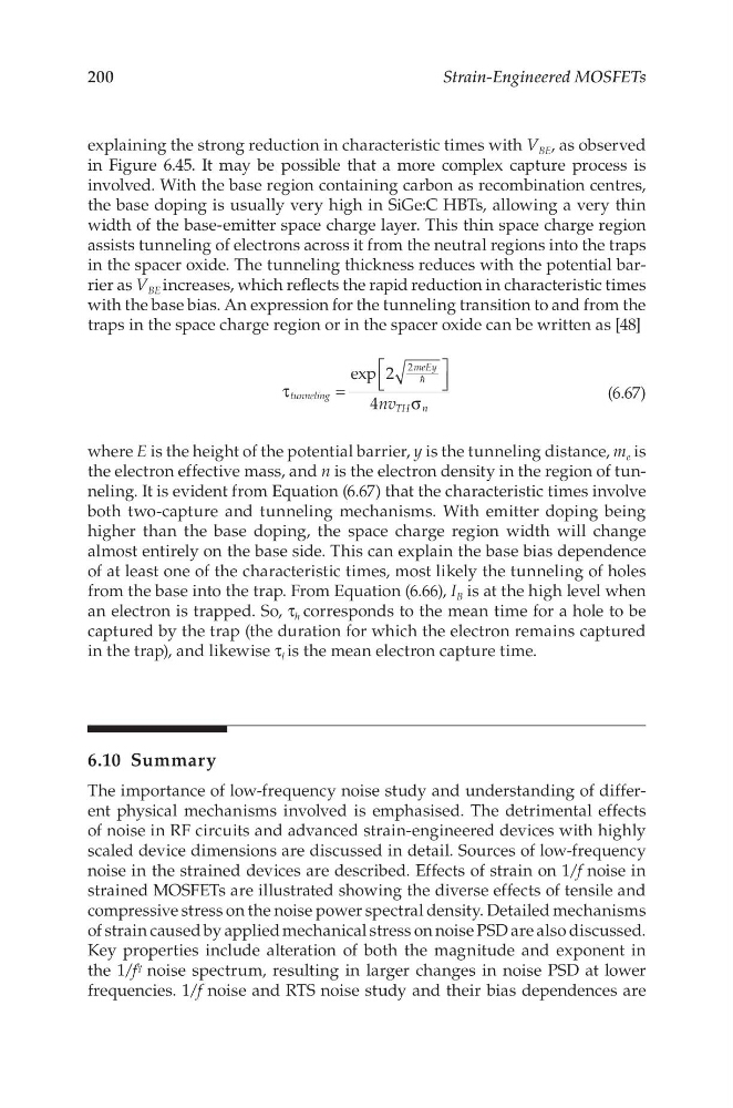
with the base bias. An expression for the tunneling transition to and from the
traps in the space charge region or in the spacer oxide can be written as [48]
nv
exp 2
4
tunneling
meEy
TH n
2
τ
=
σ
(6.67)
where E is the height of the potential barrier, y is the tunneling distance, m e is
the electron effective mass, and n is the electron density in the region of tunneling. It is evident from Equation (6.67) that the characteristic times involve
both two-capture and tunneling mechanisms. With emitter doping being
higher than the base doping, the space charge region width will change
almost entirely on the base side. This can explain the base bias dependence
of at least one of the characteristic times, most likely the tunneling of holes
from the base into the trap. From Equation (6.66), I B is at the high level when
an electron is trapped. So, τ h corresponds to the mean time for a hole to be
captured by the trap (the duration for which the electron remains captured
in the trap), and likewise τ l is the mean electron capture time.
6.10 Summary
The importance of low-frequency noise study and understanding of different physical mechanisms involved is emphasised. The detrimental effects
of noise in RF circuits and advanced strain-engineered devices with highly
scaled device dimensions are discussed in detail. Sources of low-frequency
noise in the strained devices are described. Effects of strain on 1/f noise in
strained MOSFETs are illustrated showing the diverse effects of tensile and
compressive stress on the noise power spectral density. Detailed mechanisms
of strain caused by applied mechanical stress on noise PSD are also discussed.
Key properties include alteration of both the magnitude and exponent in
the 1/f γ noise spectrum, resulting in larger changes in noise PSD at lower
frequencies. 1/f noise and RTS noise study and their bias dependences are
Strain-Engineered MOSFETs
explaining the strong reduction in characteristic times with V BE , as observed
in Figure 6.45. It may be possible that a more complex capture process is
involved. With the base region containing carbon as recombination centres,
the base doping is usually very high in SiGe:C HBTs, allowing a very thin
width of the base-emitter space charge layer. This thin space charge region
assists tunneling of electrons across it from the neutral regions into the traps
in the spacer oxide. The tunneling thickness reduces with the potential barrier as V BE increases, which reflects the rapid reduction in characteristic times
with the base bias. An expression for the tunneling transition to and from the
traps in the space charge region or in the spacer oxide can be written as [48]
nv
exp 2
4
tunneling
meEy
TH n
2
τ
=
σ
(6.67)
where E is the height of the potential barrier, y is the tunneling distance, m e is
the electron effective mass, and n is the electron density in the region of tunneling. It is evident from Equation (6.67) that the characteristic times involve
both two-capture and tunneling mechanisms. With emitter doping being
higher than the base doping, the space charge region width will change
almost entirely on the base side. This can explain the base bias dependence
of at least one of the characteristic times, most likely the tunneling of holes
from the base into the trap. From Equation (6.66), I B is at the high level when
an electron is trapped. So, τ h corresponds to the mean time for a hole to be
captured by the trap (the duration for which the electron remains captured
in the trap), and likewise τ l is the mean electron capture time.
6.10 Summary
The importance of low-frequency noise study and understanding of different physical mechanisms involved is emphasised. The detrimental effects
of noise in RF circuits and advanced strain-engineered devices with highly
scaled device dimensions are discussed in detail. Sources of low-frequency
noise in the strained devices are described. Effects of strain on 1/f noise in
strained MOSFETs are illustrated showing the diverse effects of tensile and
compressive stress on the noise power spectral density. Detailed mechanisms
of strain caused by applied mechanical stress on noise PSD are also discussed.
Key properties include alteration of both the magnitude and exponent in
the 1/f γ noise spectrum, resulting in larger changes in noise PSD at lower
frequencies. 1/f noise and RTS noise study and their bias dependences are