

198
Strain-Engineered MOSFETs
on local voltage barrier fluctuations in the emitter-base space charge region
due to trapping/de-trapping of carriers as suggested by [48]. A trapped electron in the base side causes voltage barrier height across the space charge
region ΔV BE to reduce, which increases the base current level. RTS amplitude is given by [49]
I
L
A
I
q V
kT
exp
B
S
E
B
BE
2
0
=
(6.66)
where L S is the screening length, I B0 is the initial base current level, and A E is
the emitter area.
The traps in the thin oxide at the emitter interface are dominant noise
sources for the low-frequency noise. The RTS amplitude due to these traps
scales with the injected hole current (~exp(qV BE /kT)) and is relatively small.
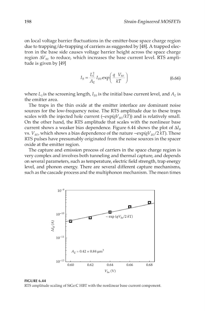
On the other hand, the RTS amplitude that scales with the nonlinear base
current shows a weaker bias dependence. Figure 6.44 shows the plot of ΔI B
vs. V BE , which shows a bias dependence of the nature ~exp(qV BE /2 kT). These
RTS pulses have presumably originated from the noise sources in the spacer
oxide at the emitter region.
The capture and emission process of carriers in the space charge region is
very complex and involves both tunneling and thermal capture, and depends
on several parameters, such as temperature, electric field strength, trap energy
level, and phonon energy. There are several different capture mechanisms,
such as the cascade process and the multiphonon mechanism. The mean times
10
–9
10
–10
∆I
B (A)
10
–11
10
–12
0.60
0.62
0.64
0.66
0.68
V be (V)
~ exp (qV be /2 kT)
A E = 0.42 × 0.84 µm
2
FIGURE 6.44
RTS amplitude scaling of SiGe:C HBT with the nonlinear base current component.
Strain-Engineered MOSFETs
on local voltage barrier fluctuations in the emitter-base space charge region
due to trapping/de-trapping of carriers as suggested by [48]. A trapped electron in the base side causes voltage barrier height across the space charge
region ΔV BE to reduce, which increases the base current level. RTS amplitude is given by [49]
I
L
A
I
q V
kT
exp
B
S
E
B
BE
2
0
=
(6.66)
where L S is the screening length, I B0 is the initial base current level, and A E is
the emitter area.
The traps in the thin oxide at the emitter interface are dominant noise
sources for the low-frequency noise. The RTS amplitude due to these traps
scales with the injected hole current (~exp(qV BE /kT)) and is relatively small.
On the other hand, the RTS amplitude that scales with the nonlinear base
current shows a weaker bias dependence. Figure 6.44 shows the plot of ΔI B
vs. V BE , which shows a bias dependence of the nature ~exp(qV BE /2 kT). These
RTS pulses have presumably originated from the noise sources in the spacer
oxide at the emitter region.
The capture and emission process of carriers in the space charge region is
very complex and involves both tunneling and thermal capture, and depends
on several parameters, such as temperature, electric field strength, trap energy
level, and phonon energy. There are several different capture mechanisms,
such as the cascade process and the multiphonon mechanism. The mean times
10
–9
10
–10
∆I
B (A)
10
–11
10
–12
0.60
0.62
0.64
0.66
0.68
V be (V)
~ exp (qV be /2 kT)
A E = 0.42 × 0.84 µm
2
FIGURE 6.44
RTS amplitude scaling of SiGe:C HBT with the nonlinear base current component.