

186
Strain-Engineered MOSFETs
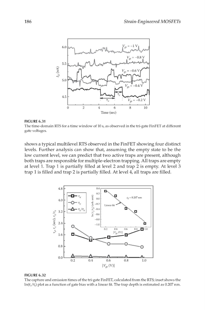
shows a typical multilevel RTS observed in the FinFET showing four distinct
levels. Further analysis can show that, assuming the empty state to be the
low current level, we can predict that two active traps are present, although
both traps are responsible for multiple-electron trapping. All traps are empty
at level 1. Trap 1 is partially filled at level 2 and trap 2 is empty. At level 3
trap 1 is filled and trap 2 is partially filled. At level 4, all traps are filled.
6.0
V gs = –1 V
V gs = –0.8 V
V gs = –0.6 V
V gs = –0.4 V
V gs = –0.2 V
τ e
τ c
5.5
I
D (nA)
5.0
4.5
0
2
4
6
Time (sec)
8
1 0
FIGURE 6.31
The time-domain RTS for a time window of 10 s, as observed in the tri-gate FinFET at different
gate voltages.
0.2
0.0
0.8
1.6
2.4
τ
e , τ
c (sec), τ
c /τ
e
In (τ
c /τ
e ) (arb. unit)
τ e
τ c
τ c /τ e
3.2
4.0
4.8
0.4
0.2
Linear t
z t = 0.207 nm
0.4
0.4
0.2
0.0
–0.2
–0.4
–0.6
–0.8
–1.0
|V gs (V)|
0.6
0.8
1.0
0.6
|V gs (V)|
0.8
1.0
FIGURE 6.32
The capture and emission times of the tri-gate FinFET, calculated from the RTS; inset shows the
ln(τ c /τ e ) plot as a function of gate bias with a linear fit. The trap depth is estimated as 0.207 nm.
Strain-Engineered MOSFETs
shows a typical multilevel RTS observed in the FinFET showing four distinct
levels. Further analysis can show that, assuming the empty state to be the
low current level, we can predict that two active traps are present, although
both traps are responsible for multiple-electron trapping. All traps are empty
at level 1. Trap 1 is partially filled at level 2 and trap 2 is empty. At level 3
trap 1 is filled and trap 2 is partially filled. At level 4, all traps are filled.
6.0
V gs = –1 V
V gs = –0.8 V
V gs = –0.6 V
V gs = –0.4 V
V gs = –0.2 V
τ e
τ c
5.5
I
D (nA)
5.0
4.5
0
2
4
6
Time (sec)
8
1 0
FIGURE 6.31
The time-domain RTS for a time window of 10 s, as observed in the tri-gate FinFET at different
gate voltages.
0.2
0.0
0.8
1.6
2.4
τ
e , τ
c (sec), τ
c /τ
e
In (τ
c /τ
e ) (arb. unit)
τ e
τ c
τ c /τ e
3.2
4.0
4.8
0.4
0.2
Linear t
z t = 0.207 nm
0.4
0.4
0.2
0.0
–0.2
–0.4
–0.6
–0.8
–1.0
|V gs (V)|
0.6
0.8
1.0
0.6
|V gs (V)|
0.8
1.0
FIGURE 6.32
The capture and emission times of the tri-gate FinFET, calculated from the RTS; inset shows the
ln(τ c /τ e ) plot as a function of gate bias with a linear fit. The trap depth is estimated as 0.207 nm.