

182
Strain-Engineered MOSFETs
to the threshold voltage) may disturb the normal switching behaviours
and circuit performance. SNWTs have also been widely studied as chemical and biochemical sensors [41, 42]. Biosensing by SNWTs is based on the
pronounced conductance changes induced by the depletion of charge carriers in the silicon body when the charged biomolecules are bound to its
surface. The high noise level in the depletion (subthreshold) region may lead
to reduced signal-to-noise ratios in these sensors. This section will present
low-frequency noise studied in MG and GAA devices.
6.7.1 Noise in Tri-Gate FinFET
The p-type tri-gate FinFET device was fabricated on a 1,000 Ǻ SOI layer.
The FinFET device has a fin height of 30 nm. The fin width and fin length
are varied from 60 to 90 nm and 60 nm to 100 μm, respectively. A 50 Ǻ SiO 2
gate oxide is grown. A polysilicon gate was deposited of thickness 1,500 Ǻ,
followed by pocket implantation and a 300 Ǻ SiO 2 spacer deposition. A deep
source/drain implant is followed. Silicidation is done for contact formation
by 300 Ǻ Ni/400 Ǻ TiN depositions with RTA at 550–600°C for 1 min. Seven
hundred angstroms of 1 μm thick Al pad is deposited for contact formation.
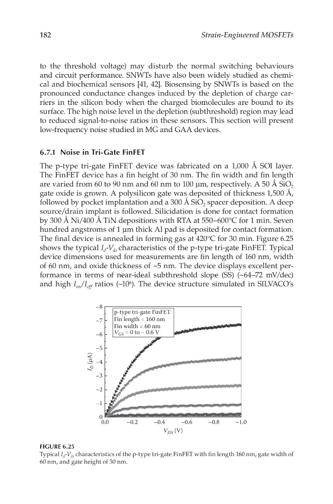
The final device is annealed in forming gas at 420°C for 30 min. Figure 6.25
shows the typical I d -V ds characteristics of the p-type tri-gate FinFET. Typical
device dimensions used for measurements are fin length of 160 nm, width
of 60 nm, and oxide thickness of ~5 nm. The device displays excellent performance in terms of near-ideal subthreshold slope (SS) (~64–72 mV/dec)
and high I on /I off ratios (~10 6 ). The device structure simulated in SILVACO’s
V DS (V)
I
D (µA)
0.0
0
–1
–2
–3
–4
–5
–6
–7
–8
p-type tri-gate FinFET
Fin length = 160 nm
Fin width = 60 nm
V GS = 0 to – 0.6 V
–0.2
–0.4
–0.6
–0.8
–1.0
FIGURE 6.25
Typical I d -V ds characteristics of the p-type tri-gate FinFET with fin length 160 nm, gate width of
60 nm, and gate height of 30 nm.
Strain-Engineered MOSFETs
to the threshold voltage) may disturb the normal switching behaviours
and circuit performance. SNWTs have also been widely studied as chemical and biochemical sensors [41, 42]. Biosensing by SNWTs is based on the
pronounced conductance changes induced by the depletion of charge carriers in the silicon body when the charged biomolecules are bound to its
surface. The high noise level in the depletion (subthreshold) region may lead
to reduced signal-to-noise ratios in these sensors. This section will present
low-frequency noise studied in MG and GAA devices.
6.7.1 Noise in Tri-Gate FinFET
The p-type tri-gate FinFET device was fabricated on a 1,000 Ǻ SOI layer.
The FinFET device has a fin height of 30 nm. The fin width and fin length
are varied from 60 to 90 nm and 60 nm to 100 μm, respectively. A 50 Ǻ SiO 2
gate oxide is grown. A polysilicon gate was deposited of thickness 1,500 Ǻ,
followed by pocket implantation and a 300 Ǻ SiO 2 spacer deposition. A deep
source/drain implant is followed. Silicidation is done for contact formation
by 300 Ǻ Ni/400 Ǻ TiN depositions with RTA at 550–600°C for 1 min. Seven
hundred angstroms of 1 μm thick Al pad is deposited for contact formation.
The final device is annealed in forming gas at 420°C for 30 min. Figure 6.25
shows the typical I d -V ds characteristics of the p-type tri-gate FinFET. Typical
device dimensions used for measurements are fin length of 160 nm, width
of 60 nm, and oxide thickness of ~5 nm. The device displays excellent performance in terms of near-ideal subthreshold slope (SS) (~64–72 mV/dec)
and high I on /I off ratios (~10 6 ). The device structure simulated in SILVACO’s
V DS (V)
I
D (µA)
0.0
0
–1
–2
–3
–4
–5
–6
–7
–8
p-type tri-gate FinFET
Fin length = 160 nm
Fin width = 60 nm
V GS = 0 to – 0.6 V
–0.2
–0.4
–0.6
–0.8
–1.0
FIGURE 6.25
Typical I d -V ds characteristics of the p-type tri-gate FinFET with fin length 160 nm, gate width of
60 nm, and gate height of 30 nm.