

181
Noise in Strain-Engineered Devices
The n-MOSFETs in this study were fabricated in the Si CMOS process.
The strained Si n-MOSFET substrate was 1.5 μm Si (100), 75 nm completely
relaxed (19% Ge) with 800 nm graded SiGe buffer and epitaxially grown
ultra-thin (150–200 Ǻ) strained Si layer. A boron well implant of dose 2 × 10 12
is used with energy 120 keV. A channel implant of dose 2 × 10 12 and energy 20
keV is used. About 3.5 nm gate oxide is thermally grown on strained Si layer.
Polysilicon gate is deposited of thickness ~4,000 Ǻ. POCl 3 dopant diffusion
is done for 60 min at 800˚C. RTA is done at 950˚C for 1 s, followed by surface
cleaning with HF:H 2 O for 10 s. The shallow S/D arsenic implant is done with
a dose of 2 × 10 15 at 15 keV. Body contact implant of BF 2 is done at 25 keV with
a dose of 3 × 10 15 . Finally, the gate metal contact Ti/TiN/AlSiCu of thickness 8,500 Ǻ is deposited, thus forming a Si/strained Si/relaxed SiGe MOS
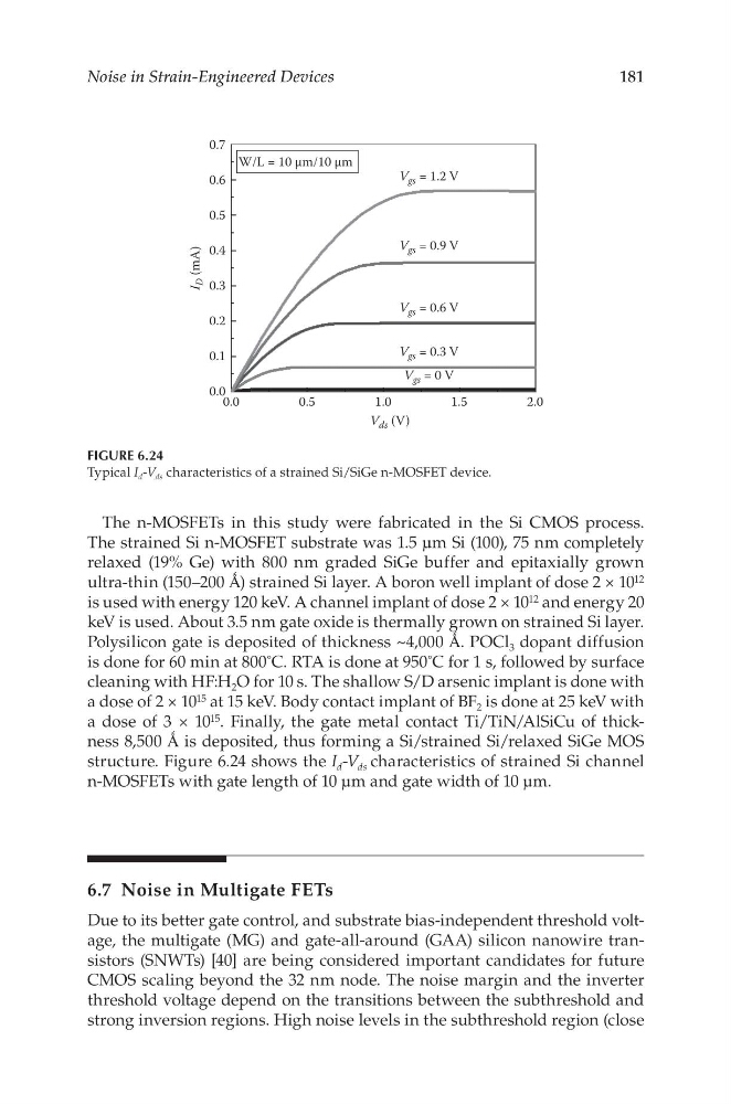
structure. Figure 6.24 shows the I d -V ds characteristics of strained Si channel
n-MOSFETs with gate length of 10 μm and gate width of 10 μm.
6.7 Noise in Multigate FETs
Due to its better gate control, and substrate bias-independent threshold voltage, the multigate (MG) and gate-all-around (GAA) silicon nanowire transistors (SNWTs) [40] are being considered important candidates for future
CMOS scaling beyond the 32 nm node. The noise margin and the inverter
threshold voltage depend on the transitions between the subthreshold and
strong inversion regions. High noise levels in the subthreshold region (close
0.7
0.6
0.5
0.4
0.3
I
D (mA)
0.2
0.1
0.0
0.0
0.5
W/L = 10 µm/10 µm
V ds (V)
V gs = 0.3 V
V gs = 0 V
V gs = 0.6 V
V gs = 0.9 V
V gs = 1.2 V
1.0
1.5
2.0
FIGURE 6.24
Typical I d -V ds characteristics of a strained Si/SiGe n-MOSFET device.
Noise in Strain-Engineered Devices
The n-MOSFETs in this study were fabricated in the Si CMOS process.
The strained Si n-MOSFET substrate was 1.5 μm Si (100), 75 nm completely
relaxed (19% Ge) with 800 nm graded SiGe buffer and epitaxially grown
ultra-thin (150–200 Ǻ) strained Si layer. A boron well implant of dose 2 × 10 12
is used with energy 120 keV. A channel implant of dose 2 × 10 12 and energy 20
keV is used. About 3.5 nm gate oxide is thermally grown on strained Si layer.
Polysilicon gate is deposited of thickness ~4,000 Ǻ. POCl 3 dopant diffusion
is done for 60 min at 800˚C. RTA is done at 950˚C for 1 s, followed by surface
cleaning with HF:H 2 O for 10 s. The shallow S/D arsenic implant is done with
a dose of 2 × 10 15 at 15 keV. Body contact implant of BF 2 is done at 25 keV with
a dose of 3 × 10 15 . Finally, the gate metal contact Ti/TiN/AlSiCu of thickness 8,500 Ǻ is deposited, thus forming a Si/strained Si/relaxed SiGe MOS
structure. Figure 6.24 shows the I d -V ds characteristics of strained Si channel
n-MOSFETs with gate length of 10 μm and gate width of 10 μm.
6.7 Noise in Multigate FETs
Due to its better gate control, and substrate bias-independent threshold voltage, the multigate (MG) and gate-all-around (GAA) silicon nanowire transistors (SNWTs) [40] are being considered important candidates for future
CMOS scaling beyond the 32 nm node. The noise margin and the inverter
threshold voltage depend on the transitions between the subthreshold and
strong inversion regions. High noise levels in the subthreshold region (close
0.7
0.6
0.5
0.4
0.3
I
D (mA)
0.2
0.1
0.0
0.0
0.5
W/L = 10 µm/10 µm
V ds (V)
V gs = 0.3 V
V gs = 0 V
V gs = 0.6 V
V gs = 0.9 V
V gs = 1.2 V
1.0
1.5
2.0
FIGURE 6.24
Typical I d -V ds characteristics of a strained Si/SiGe n-MOSFET device.