

174
Strain-Engineered MOSFETs
where N E kT
( )
T
F
is the interface state density (D it ) per unit energy at the Fermi
energy level, and λ is McWhorter’s tunneling parameter [35]. Increasing gate
bias increases the number of active traps, and therefore increases the noise
level. Variability of 1/f noise is largely due to the statistics of trap density
and location. It was proposed that at low bias, nonuniform carrier densities
can be formed, resulting in a change of current path and increased noise
variability. The general model for describing a relation between inversion
charge, N inv , and the Coulomb scattering parameter for the contribution to
mobility fluctuation of the charged traps, α sc (with α sc,i being the contribution
of the ith trap and μ c0 is 5.9 × 10 8 cm/Vs), is given as
N
N
1
1
sc
T
sc i
i
N
c
i nv
,
1
0
T
∑
α =
α = µ
=
(6.51)
As gate voltage is increased, inversion charge, N inv , grows and becomes
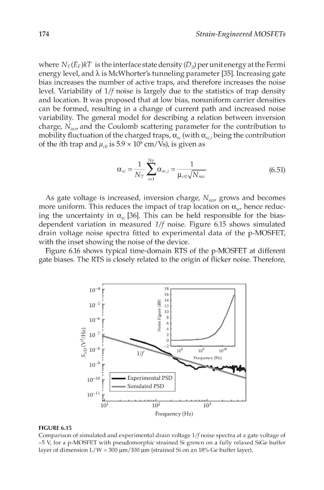
more uniform. This reduces the impact of trap location on α sc , hence reducing the uncertainty in α sc [36]. This can be held responsible for the biasdependent variation in measured 1/f noise. Figure 6.15 shows simulated
drain voltage noise spectra fitted to experimental data of the p-MOSFET,
with the inset showing the noise of the device.
Figure 6.16 shows typical time-domain RTS of the p-MOSFET at different
gate biases. The RTS is closely related to the origin of flicker noise. Therefore,
10
–4
10
–5
10
–6
10
–7
S
VD (V
2
/Hz)
10
–8
10
8
–2
0
Frequency (Hz)
2
4
6
Noise Figure (dB)
8
10
12
14
16
18
10
9
10
10
10
–9
Experimental PSD
1/f
Simulated PSD
10 –10
10
–11
10
1
10
2
Frequency (Hz)
10
3
FIGURE 6.15
Comparison of simulated and experimental drain voltage 1/f noise spectra at a gate voltage of
–5 V, for a p-MOSFET with pseudomorphic strained Si grown on a fully relaxed SiGe buffer
layer of dimension L/W = 300 μm/100 μm (strained Si on an 18% Ge buffer layer).
Strain-Engineered MOSFETs
where N E kT
( )
T
F
is the interface state density (D it ) per unit energy at the Fermi
energy level, and λ is McWhorter’s tunneling parameter [35]. Increasing gate
bias increases the number of active traps, and therefore increases the noise
level. Variability of 1/f noise is largely due to the statistics of trap density
and location. It was proposed that at low bias, nonuniform carrier densities
can be formed, resulting in a change of current path and increased noise
variability. The general model for describing a relation between inversion
charge, N inv , and the Coulomb scattering parameter for the contribution to
mobility fluctuation of the charged traps, α sc (with α sc,i being the contribution
of the ith trap and μ c0 is 5.9 × 10 8 cm/Vs), is given as
N
N
1
1
sc
T
sc i
i
N
c
i nv
,
1
0
T
∑
α =
α = µ
=
(6.51)
As gate voltage is increased, inversion charge, N inv , grows and becomes
more uniform. This reduces the impact of trap location on α sc , hence reducing the uncertainty in α sc [36]. This can be held responsible for the biasdependent variation in measured 1/f noise. Figure 6.15 shows simulated
drain voltage noise spectra fitted to experimental data of the p-MOSFET,
with the inset showing the noise of the device.
Figure 6.16 shows typical time-domain RTS of the p-MOSFET at different
gate biases. The RTS is closely related to the origin of flicker noise. Therefore,
10
–4
10
–5
10
–6
10
–7
S
VD (V
2
/Hz)
10
–8
10
8
–2
0
Frequency (Hz)
2
4
6
Noise Figure (dB)
8
10
12
14
16
18
10
9
10
10
10
–9
Experimental PSD
1/f
Simulated PSD
10 –10
10
–11
10
1
10
2
Frequency (Hz)
10
3
FIGURE 6.15
Comparison of simulated and experimental drain voltage 1/f noise spectra at a gate voltage of
–5 V, for a p-MOSFET with pseudomorphic strained Si grown on a fully relaxed SiGe buffer
layer of dimension L/W = 300 μm/100 μm (strained Si on an 18% Ge buffer layer).