

173
Noise in Strain-Engineered Devices
biasing network and supplying appropriate drain and gate bias using the
Easy-Expert software. The minute fluctuations in the drain/source voltage
were amplified to the measurable range using low-noise SR570 preamplifier operating in the 0.03 Hz–300 kHz range with voltage gain set to 1,000.
In order to obtain a stable spectrum, the number of averages was set at 30
and a 90% sampling window overlap was used for optimal real-time processing. A computer interface was provided through a General Purpose
Interface Bus (GPIB) connection to control the dynamic signal analyser and
automate the noise data collection.
6.6.2 Strained Si MOSFETs
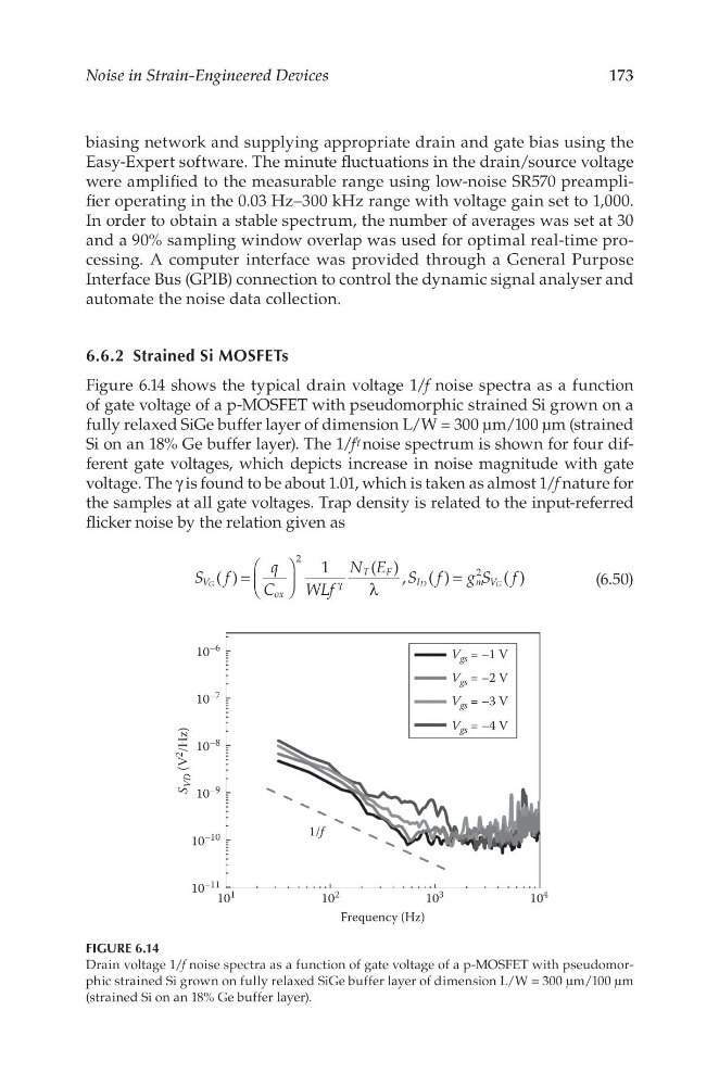
Figure 6.14 shows the typical drain voltage 1/f noise spectra as a function
of gate voltage of a p-MOSFET with pseudomorphic strained Si grown on a
fully relaxed SiGe buffer layer of dimension L/W = 300 μm/100 μm (strained
Si on an 18% Ge buffer layer). The 1/f γ noise spectrum is shown for four different gate voltages, which depicts increase in noise magnitude with gate
voltage. The γ is found to be about 1.01, which is taken as almost 1/f nature for
the samples at all gate voltages. Trap density is related to the input-referred
flicker noise by the relation given as
S f
q
C
WLf
N E S f
g S f
( )
1
( ) , ( )
( )
V
ox
T
F
I
mV
2
2
G
D
G
=
λ
=
γ
(6.50)
10
–6
10
–7
10
–8
S
VD (V
2
/Hz)
10 –9
10
–10
10
–11
10
1
10
2
1/f
V gs = –1 V
V gs = –2 V
V gs = –3 V
V gs = –4 V
10
3
Frequency (Hz)
10
4
FIGURE 6.14
Drain voltage 1/f noise spectra as a function of gate voltage of a p-MOSFET with pseudomorphic strained Si grown on fully relaxed SiGe buffer layer of dimension L/W = 300 μm/100 μm
(strained Si on an 18% Ge buffer layer).
Noise in Strain-Engineered Devices
biasing network and supplying appropriate drain and gate bias using the
Easy-Expert software. The minute fluctuations in the drain/source voltage
were amplified to the measurable range using low-noise SR570 preamplifier operating in the 0.03 Hz–300 kHz range with voltage gain set to 1,000.
In order to obtain a stable spectrum, the number of averages was set at 30
and a 90% sampling window overlap was used for optimal real-time processing. A computer interface was provided through a General Purpose
Interface Bus (GPIB) connection to control the dynamic signal analyser and
automate the noise data collection.
6.6.2 Strained Si MOSFETs
Figure 6.14 shows the typical drain voltage 1/f noise spectra as a function
of gate voltage of a p-MOSFET with pseudomorphic strained Si grown on a
fully relaxed SiGe buffer layer of dimension L/W = 300 μm/100 μm (strained
Si on an 18% Ge buffer layer). The 1/f γ noise spectrum is shown for four different gate voltages, which depicts increase in noise magnitude with gate
voltage. The γ is found to be about 1.01, which is taken as almost 1/f nature for
the samples at all gate voltages. Trap density is related to the input-referred
flicker noise by the relation given as
S f
q
C
WLf
N E S f
g S f
( )
1
( ) , ( )
( )
V
ox
T
F
I
mV
2
2
G
D
G
=
λ
=
γ
(6.50)
10
–6
10
–7
10
–8
S
VD (V
2
/Hz)
10 –9
10
–10
10
–11
10
1
10
2
1/f
V gs = –1 V
V gs = –2 V
V gs = –3 V
V gs = –4 V
10
3
Frequency (Hz)
10
4
FIGURE 6.14
Drain voltage 1/f noise spectra as a function of gate voltage of a p-MOSFET with pseudomorphic strained Si grown on fully relaxed SiGe buffer layer of dimension L/W = 300 μm/100 μm
(strained Si on an 18% Ge buffer layer).