

172
Strain-Engineered MOSFETs
and low power. However, the 1/f noise of the MOS transistors is a problem
that must be taken care of. With downscaling of device dimensions 1/f noise
increases, which makes it extremely important not only to understand the
origin of the noise, but also to reduce the noise magnitude for accurate detection of the desired signal. The 1/f noise is sensitive to technology; the choice
of gate oxide material and oxidation/deposition process, as well as channel type and material, can have a large impact on the noise performance.
The trap density and Hooge parameter can both be used as figures of merit
for the 1/f noise performance, irrespective of the origin of the noise. In this
section, low-frequency noise in advanced and highly scaled MOS transistor
architectures is discussed.
6.6.1 Low-Frequency Noise Measurements
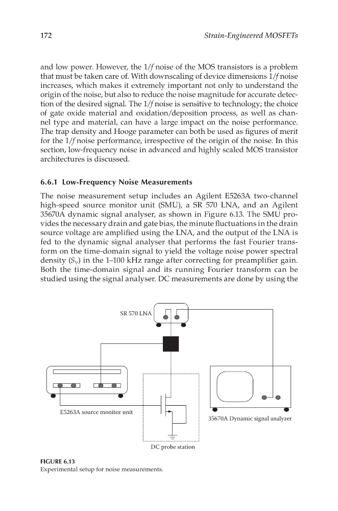
The noise measurement setup includes an Agilent E5263A two-channel
high-speed source monitor unit (SMU), a SR 570 LNA, and an Agilent
35670A dynamic signal analyser, as shown in Figure 6.13. The SMU provides the necessary drain and gate bias, the minute fluctuations in the drain
source voltage are amplified using the LNA, and the output of the LNA is
fed to the dynamic signal analyser that performs the fast Fourier transform on the time-domain signal to yield the voltage noise power spectral
density (S V ) in the 1–100 kHz range after correcting for preamplifier gain.
Both the time-domain signal and its running Fourier transform can be
studied using the signal analyser. DC measurements are done by using the
SR 570 LNA
E5263A source monitor unit
35670A Dynamic signal analyzer
DC probe station
FIGURE 6.13
Experimental setup for noise measurements.
Strain-Engineered MOSFETs
and low power. However, the 1/f noise of the MOS transistors is a problem
that must be taken care of. With downscaling of device dimensions 1/f noise
increases, which makes it extremely important not only to understand the
origin of the noise, but also to reduce the noise magnitude for accurate detection of the desired signal. The 1/f noise is sensitive to technology; the choice
of gate oxide material and oxidation/deposition process, as well as channel type and material, can have a large impact on the noise performance.
The trap density and Hooge parameter can both be used as figures of merit
for the 1/f noise performance, irrespective of the origin of the noise. In this
section, low-frequency noise in advanced and highly scaled MOS transistor
architectures is discussed.
6.6.1 Low-Frequency Noise Measurements
The noise measurement setup includes an Agilent E5263A two-channel
high-speed source monitor unit (SMU), a SR 570 LNA, and an Agilent
35670A dynamic signal analyser, as shown in Figure 6.13. The SMU provides the necessary drain and gate bias, the minute fluctuations in the drain
source voltage are amplified using the LNA, and the output of the LNA is
fed to the dynamic signal analyser that performs the fast Fourier transform on the time-domain signal to yield the voltage noise power spectral
density (S V ) in the 1–100 kHz range after correcting for preamplifier gain.
Both the time-domain signal and its running Fourier transform can be
studied using the signal analyser. DC measurements are done by using the
SR 570 LNA
E5263A source monitor unit
35670A Dynamic signal analyzer
DC probe station
FIGURE 6.13
Experimental setup for noise measurements.