

171
Noise in Strain-Engineered Devices
expression is valid for a low drain bias [24]. Equation (6.47) can be rewritten
for applied mechanical stress, using Equation (6.45),
S f
WL
I
N
q
N
f
f
dE
q V
t
z
f
dz
( ; )
( )
( )exp[ ( )
( )] 4 ( ) ( )(1
( ))
.
( )exp[( ( ) | |/
( )). ]
1 (2 ( ))
I
D
B
t
t
t
E
E
ox
ox
t
2
2
2
0
2
0
D
Vox
Cox
ox
∫
∫
σ =
σ κ σ
−ξ σ Φ σ
σ σ − σ
τ σ
ξ σ
+ η σ
+ π τ σ
(6.48)
where
f
E E
q
kT
and
z
( ) 1 exp
( )
, ( )
exp[ / ( )]
t
Fn
B
1
0
σ = +
−
− Φ σ
τ σ = τ
λ σ
−
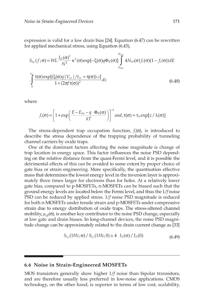
The stress-dependent trap occupation function, f t (σ), is introduced to
describe the stress dependence of the trapping probability of tunneling
channel carriers by oxide traps.
One of the dominant factors affecting the noise magnitude is change of
trap location in energy space. This factor influences the noise PSD depending on the relative distance from the quasi-Fermi level, and it is possible the
detrimental effects of this can be avoided to some extent by proper choice of
gate bias or strain engineering. More specifically, the quantisation effective
mass that determines the lowest energy level in the inversion layer is approximately three times larger for electrons than for holes. At a relatively lower
gate bias, compared to p-MOSFETs, n-MOSFETs can be biased such that the
ground energy levels are located below the Fermi level, and thus the 1/f noise
PSD can be reduced by applied stress. 1/f noise PSD magnitude is reduced
for both n-MOSFETs under tensile strain and p-MOSFETs under compressive
strain due to energy distribution of oxide traps. The stress-altered channel
mobility, μ eff (σ), is another key contributor to the noise PSD change, especially
at low gate and drain biases. In long-channel devices, the noise PSD magnitude change can be approximately related to the drain current change as [33]
S
Hz
S
Hz
I
I
(1 ; )/ (1 ;0) 4
( )/ (0)
I
I
D
D
D
D
σ
≅
σ
(6.49)
6.6 Noise in Strain-Engineered MOSFETs
MOS transistors generally show higher 1/f noise than bipolar transistors,
and are therefore usually less preferred in low-noise applications. CMOS
technology, on the other hand, is superior in terms of low cost, scalability,
Noise in Strain-Engineered Devices
expression is valid for a low drain bias [24]. Equation (6.47) can be rewritten
for applied mechanical stress, using Equation (6.45),
S f
WL
I
N
q
N
f
f
dE
q V
t
z
f
dz
( ; )
( )
( )exp[ ( )
( )] 4 ( ) ( )(1
( ))
.
( )exp[( ( ) | |/
( )). ]
1 (2 ( ))
I
D
B
t
t
t
E
E
ox
ox
t
2
2
2
0
2
0
D
Vox
Cox
ox
∫
∫
σ =
σ κ σ
−ξ σ Φ σ
σ σ − σ
τ σ
ξ σ
+ η σ
+ π τ σ
(6.48)
where
f
E E
q
kT
and
z
( ) 1 exp
( )
, ( )
exp[ / ( )]
t
Fn
B
1
0
σ = +
−
− Φ σ
τ σ = τ
λ σ
−
The stress-dependent trap occupation function, f t (σ), is introduced to
describe the stress dependence of the trapping probability of tunneling
channel carriers by oxide traps.
One of the dominant factors affecting the noise magnitude is change of
trap location in energy space. This factor influences the noise PSD depending on the relative distance from the quasi-Fermi level, and it is possible the
detrimental effects of this can be avoided to some extent by proper choice of
gate bias or strain engineering. More specifically, the quantisation effective
mass that determines the lowest energy level in the inversion layer is approximately three times larger for electrons than for holes. At a relatively lower
gate bias, compared to p-MOSFETs, n-MOSFETs can be biased such that the
ground energy levels are located below the Fermi level, and thus the 1/f noise
PSD can be reduced by applied stress. 1/f noise PSD magnitude is reduced
for both n-MOSFETs under tensile strain and p-MOSFETs under compressive
strain due to energy distribution of oxide traps. The stress-altered channel
mobility, μ eff (σ), is another key contributor to the noise PSD change, especially
at low gate and drain biases. In long-channel devices, the noise PSD magnitude change can be approximately related to the drain current change as [33]
S
Hz
S
Hz
I
I
(1 ; )/ (1 ;0) 4
( )/ (0)
I
I
D
D
D
D
σ
≅
σ
(6.49)
6.6 Noise in Strain-Engineered MOSFETs
MOS transistors generally show higher 1/f noise than bipolar transistors,
and are therefore usually less preferred in low-noise applications. CMOS
technology, on the other hand, is superior in terms of low cost, scalability,