

170
Strain-Engineered MOSFETs
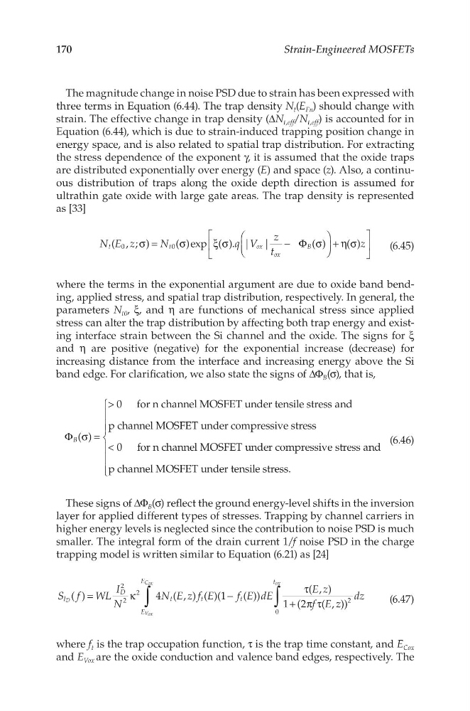
The magnitude change in noise PSD due to strain has been expressed with
three terms in Equation (6.44). The trap density N t (E Fn ) should change with
strain. The effective change in trap density (ΔN t,eff /N t,eff ) is accounted for in
Equation (6.44), which is due to strain-induced trapping position change in
energy space, and is also related to spatial trap distribution. For extracting
the stress dependence of the exponent γ, it is assumed that the oxide traps
are distributed exponentially over energy (E) and space (z). Also, a continuous distribution of traps along the oxide depth direction is assumed for
ultrathin gate oxide with large gate areas. The trap density is represented
as [33]
N E z
N
q V
z
t
z
( , ; )
( )exp ( ). | |
( )
( )
t
t
ox
ox
B
0
0
σ =
σ
ξσ
− Φ σ
+ η σ
(6.45)
where the terms in the exponential argument are due to oxide band bending, applied stress, and spatial trap distribution, respectively. In general, the
parameters N t0 , ξ, and η are functions of mechanical stress since applied
stress can alter the trap distribution by affecting both trap energy and existing interface strain between the Si channel and the oxide. The signs for ξ
and η are positive (negative) for the exponential increase (decrease) for
increasing distance from the interface and increasing energy above the Si
band edge. For clarification, we also state the signs of ΔΦ B (σ), that is,
( )
0 for n channel MOSFET under tensile stress and
p channel MOSFET under compressive stress
< 0 for n channel MOSFET under compressive stress and
p channel MOSFET under tensile stress.
B
Φ σ =
>
(6.46)
These signs of ΔΦ B (σ) reflect the ground energy-level shifts in the inversion
layer for applied different types of stresses. Trapping by channel carriers in
higher energy levels is neglected since the contribution to noise PSD is much
smaller. The integral form of the drain current 1/f noise PSD in the charge
trapping model is written similar to Equation (6.21) as [24]
S f WL
I
N
N E z f E
f E dE
E z
f E z
dz
( )
4 ( , ) ( )(1
( ))
( , )
1 (2 ( , ))
I
D
t
t
t
t
E
E
2
2
2
2
0
D
ox
Vox
Cox
∫
∫
=
κ
−
τ
+ π τ
(6.47)
where f t is the trap occupation function, τ is the trap time constant, and E Cox
and E Vox are the oxide conduction and valence band edges, respectively. The
Strain-Engineered MOSFETs
The magnitude change in noise PSD due to strain has been expressed with
three terms in Equation (6.44). The trap density N t (E Fn ) should change with
strain. The effective change in trap density (ΔN t,eff /N t,eff ) is accounted for in
Equation (6.44), which is due to strain-induced trapping position change in
energy space, and is also related to spatial trap distribution. For extracting
the stress dependence of the exponent γ, it is assumed that the oxide traps
are distributed exponentially over energy (E) and space (z). Also, a continuous distribution of traps along the oxide depth direction is assumed for
ultrathin gate oxide with large gate areas. The trap density is represented
as [33]
N E z
N
q V
z
t
z
( , ; )
( )exp ( ). | |
( )
( )
t
t
ox
ox
B
0
0
σ =
σ
ξσ
− Φ σ
+ η σ
(6.45)
where the terms in the exponential argument are due to oxide band bending, applied stress, and spatial trap distribution, respectively. In general, the
parameters N t0 , ξ, and η are functions of mechanical stress since applied
stress can alter the trap distribution by affecting both trap energy and existing interface strain between the Si channel and the oxide. The signs for ξ
and η are positive (negative) for the exponential increase (decrease) for
increasing distance from the interface and increasing energy above the Si
band edge. For clarification, we also state the signs of ΔΦ B (σ), that is,
( )
0 for n channel MOSFET under tensile stress and
p channel MOSFET under compressive stress
< 0 for n channel MOSFET under compressive stress and
p channel MOSFET under tensile stress.
B
Φ σ =
>
(6.46)
These signs of ΔΦ B (σ) reflect the ground energy-level shifts in the inversion
layer for applied different types of stresses. Trapping by channel carriers in
higher energy levels is neglected since the contribution to noise PSD is much
smaller. The integral form of the drain current 1/f noise PSD in the charge
trapping model is written similar to Equation (6.21) as [24]
S f WL
I
N
N E z f E
f E dE
E z
f E z
dz
( )
4 ( , ) ( )(1
( ))
( , )
1 (2 ( , ))
I
D
t
t
t
t
E
E
2
2
2
2
0
D
ox
Vox
Cox
∫
∫
=
κ
−
τ
+ π τ
(6.47)
where f t is the trap occupation function, τ is the trap time constant, and E Cox
and E Vox are the oxide conduction and valence band edges, respectively. The