

175
Noise in Strain-Engineered Devices
the voltage dependencies can be similarly explained by the increase in active
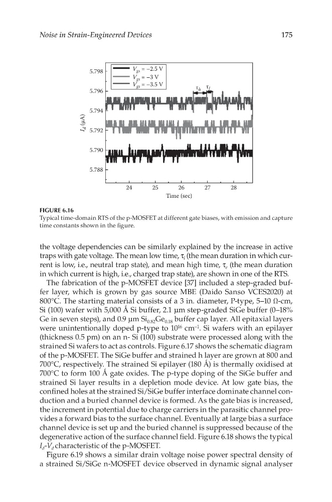
traps with gate voltage. The mean low time, τ l (the mean duration in which current is low, i.e., neutral trap state), and mean high time, τ e (the mean duration
in which current is high, i.e., charged trap state), are shown in one of the RTS.
The fabrication of the p-MOSFET device [37] included a step-graded buffer layer, which is grown by gas source MBE (Daido Sanso VCES2020) at
800°C. The starting material consists of a 3 in. diameter, P-type, 5–10 Ω-cm,
Si (100) wafer with 5,000 Ǻ Si buffer, 2.1 μm step-graded SiGe buffer (0–18%
Ge in seven steps), and 0.9 μm Si 0.82 Ge 0.18 buffer cap layer. All epitaxial layers
were unintentionally doped p-type to 10 16 cm –1 . Si wafers with an epilayer
(thickness 0.5 pm) on an n- Si (100) substrate were processed along with the
strained Si wafers to act as controls. Figure 6.17 shows the schematic diagram
of the p-MOSFET. The SiGe buffer and strained h layer are grown at 800 and
700°C, respectively. The strained Si epilayer (180 Ǻ) is thermally oxidised at
700°C to form 100 Ǻ gate oxides. The p-type doping of the SiGe buffer and
strained Si layer results in a depletion mode device. At low gate bias, the
confined holes at the strained Si/SiGe buffer interface dominate channel conduction and a buried channel device is formed. As the gate bias is increased,
the increment in potential due to charge carriers in the parasitic channel provides a forward bias to the surface channel. Eventually at large bias a surface
channel device is set up and the buried channel is suppressed because of the
degenerative action of the surface channel field. Figure 6.18 shows the typical
I d -V d characteristic of the p-MOSFET.
Figure 6.19 shows a similar drain voltage noise power spectral density of
a strained Si/SiGe n-MOSFET device observed in dynamic signal analyser
24
5.788
5.790
5.792
I
d (µA)
5.794
τ h τ l
5.796
5.798
V gs = –2.5 V
V gs = –3 V
V gs = –3.5 V
25
26
Time (sec)
27
28
FIGURE 6.16
Typical time-domain RTS of the p-MOSFET at different gate biases, with emission and capture
time constants shown in the figure.
Noise in Strain-Engineered Devices
the voltage dependencies can be similarly explained by the increase in active
traps with gate voltage. The mean low time, τ l (the mean duration in which current is low, i.e., neutral trap state), and mean high time, τ e (the mean duration
in which current is high, i.e., charged trap state), are shown in one of the RTS.
The fabrication of the p-MOSFET device [37] included a step-graded buffer layer, which is grown by gas source MBE (Daido Sanso VCES2020) at
800°C. The starting material consists of a 3 in. diameter, P-type, 5–10 Ω-cm,
Si (100) wafer with 5,000 Ǻ Si buffer, 2.1 μm step-graded SiGe buffer (0–18%
Ge in seven steps), and 0.9 μm Si 0.82 Ge 0.18 buffer cap layer. All epitaxial layers
were unintentionally doped p-type to 10 16 cm –1 . Si wafers with an epilayer
(thickness 0.5 pm) on an n- Si (100) substrate were processed along with the
strained Si wafers to act as controls. Figure 6.17 shows the schematic diagram
of the p-MOSFET. The SiGe buffer and strained h layer are grown at 800 and
700°C, respectively. The strained Si epilayer (180 Ǻ) is thermally oxidised at
700°C to form 100 Ǻ gate oxides. The p-type doping of the SiGe buffer and
strained Si layer results in a depletion mode device. At low gate bias, the
confined holes at the strained Si/SiGe buffer interface dominate channel conduction and a buried channel device is formed. As the gate bias is increased,
the increment in potential due to charge carriers in the parasitic channel provides a forward bias to the surface channel. Eventually at large bias a surface
channel device is set up and the buried channel is suppressed because of the
degenerative action of the surface channel field. Figure 6.18 shows the typical
I d -V d characteristic of the p-MOSFET.
Figure 6.19 shows a similar drain voltage noise power spectral density of
a strained Si/SiGe n-MOSFET device observed in dynamic signal analyser
24
5.788
5.790
5.792
I
d (µA)
5.794
τ h τ l
5.796
5.798
V gs = –2.5 V
V gs = –3 V
V gs = –3.5 V
25
26
Time (sec)
27
28
FIGURE 6.16
Typical time-domain RTS of the p-MOSFET at different gate biases, with emission and capture
time constants shown in the figure.