

168
Strain-Engineered MOSFETs
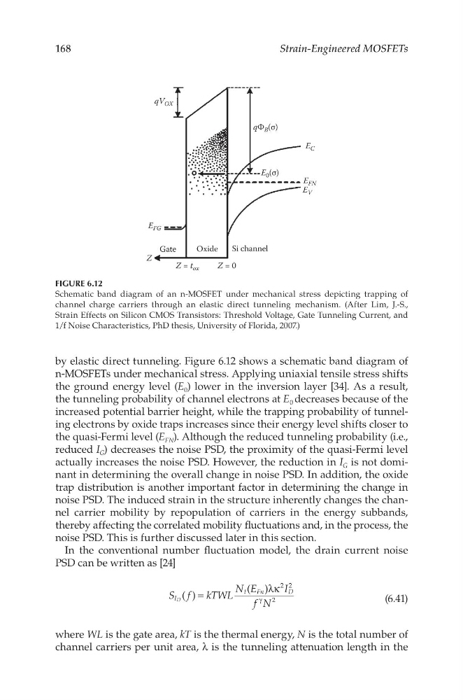
by elastic direct tunneling. Figure 6.12 shows a schematic band diagram of
n-MOSFETs under mechanical stress. Applying uniaxial tensile stress shifts
the ground energy level (E 0 ) lower in the inversion layer [34]. As a result,
the tunneling probability of channel electrons at E 0 decreases because of the
increased potential barrier height, while the trapping probability of tunneling electrons by oxide traps increases since their energy level shifts closer to
the quasi-Fermi level (E FN ). Although the reduced tunneling probability (i.e.,
reduced I G ) decreases the noise PSD, the proximity of the quasi-Fermi level
actually increases the noise PSD. However, the reduction in I G is not dominant in determining the overall change in noise PSD. In addition, the oxide
trap distribution is another important factor in determining the change in
noise PSD. The induced strain in the structure inherently changes the channel carrier mobility by repopulation of carriers in the energy subbands,
thereby affecting the correlated mobility fluctuations and, in the process, the
noise PSD. This is further discussed later in this section.
In the conventional number fluctuation model, the drain current noise
PSD can be written as [24]
S f
kTWL
N E
I
f N
( )
( )
I
t
Fn
D
2 2
2
D
=
λκ
γ
(6.41)
where WL is the gate area, kT is the thermal energy, N is the total number of
channel carriers per unit area, λ is the tunneling attenuation length in the
FIGURE 6.12
Schematic band diagram of an n-MOSFET under mechanical stress depicting trapping of
channel charge carriers through an elastic direct tunneling mechanism. (After Lim, J.-S.,
Strain Effects on Silicon CMOS Transistors: Threshold Voltage, Gate Tunneling Current, and
1/f Noise Characteristics, PhD thesis, University of Florida, 2007.)
Strain-Engineered MOSFETs
by elastic direct tunneling. Figure 6.12 shows a schematic band diagram of
n-MOSFETs under mechanical stress. Applying uniaxial tensile stress shifts
the ground energy level (E 0 ) lower in the inversion layer [34]. As a result,
the tunneling probability of channel electrons at E 0 decreases because of the
increased potential barrier height, while the trapping probability of tunneling electrons by oxide traps increases since their energy level shifts closer to
the quasi-Fermi level (E FN ). Although the reduced tunneling probability (i.e.,
reduced I G ) decreases the noise PSD, the proximity of the quasi-Fermi level
actually increases the noise PSD. However, the reduction in I G is not dominant in determining the overall change in noise PSD. In addition, the oxide
trap distribution is another important factor in determining the change in
noise PSD. The induced strain in the structure inherently changes the channel carrier mobility by repopulation of carriers in the energy subbands,
thereby affecting the correlated mobility fluctuations and, in the process, the
noise PSD. This is further discussed later in this section.
In the conventional number fluctuation model, the drain current noise
PSD can be written as [24]
S f
kTWL
N E
I
f N
( )
( )
I
t
Fn
D
2 2
2
D
=
λκ
γ
(6.41)
where WL is the gate area, kT is the thermal energy, N is the total number of
channel carriers per unit area, λ is the tunneling attenuation length in the
FIGURE 6.12
Schematic band diagram of an n-MOSFET under mechanical stress depicting trapping of
channel charge carriers through an elastic direct tunneling mechanism. (After Lim, J.-S.,
Strain Effects on Silicon CMOS Transistors: Threshold Voltage, Gate Tunneling Current, and
1/f Noise Characteristics, PhD thesis, University of Florida, 2007.)