

167
Noise in Strain-Engineered Devices
is on S f
( ; )
ID
σ and Δγ(σ), as they vary independently with applied stress.
A theoretical model for the stress dependence of drain current noise PSDs is
shown in the following section.
6.5.4 Number Fluctuation Model under Strain
6.5.4.1 Mechanisms for Change in Noise PSD under Strain
A number fluctuation model is considered to explain the strain dependence
of 1/f noise in MOSFETs. As described in Section 6.4.1, the number fluctuation model explains the origin of 1/f noise as trapping and de-trapping of
channel charge carriers by oxide traps [24]. In ultra-thin gate oxide MOSFETs,
even a relatively low gate bias can cause significant band bending in the Si
channel, thus causing the Fermi level to lie above the conduction band edge
or below the valence band edge. Due to the band bending, the 1/f noise PSD
mostly results from trapping/de-trapping of channel carriers at oxide traps
existing at an energy level above the Si conduction band edge or below the
Si valence band edge. In ultra-thin gate oxides, therefore, trapping by twostep or multiphonon processes can be neglected compared to the trapping
f = 50 Hz
7
×10
–20
6
S
ID (σ) (A
2
/Hz)
5
4
0
5 0
100
|Stress| (MPa)
(a)
150
200
f = 200 Hz
σ = –200 MPa
1.95
×10
–20
1.70
S
ID (σ) (A
2
/Hz)
1.45
1.20
0
5 0
100
|Stress| (MPa)
(b)
150
200
f = 600 Hz
9.7
×10
–21
8.8
S
ID (σ) (A
2
/Hz)
7.9
7.0
0
5 0
100
|Stress| (MPa)
(c)
150
200
–16
∆S
ID (σ)/S
ID (0) (%)
–20
–24
–28
10
1
10
2
Frequency (Hz)
(d)
10
3
10
4
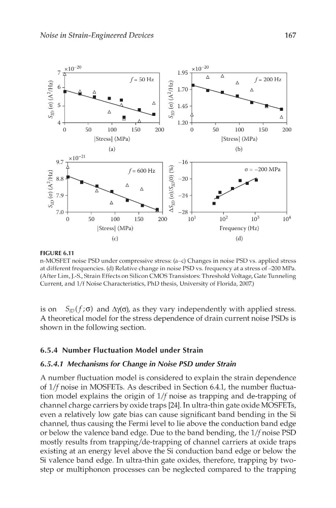
FIGURE 6.11
n-MOSFET noise PSD under compressive stress: (a–c) Changes in noise PSD vs. applied stress
at different frequencies. (d) Relative change in noise PSD vs. frequency at a stress of –200 MPa.
(After Lim, J.-S., Strain Effects on Silicon CMOS Transistors: Threshold Voltage, Gate Tunneling
Current, and 1/f Noise Characteristics, PhD thesis, University of Florida, 2007.)
Noise in Strain-Engineered Devices
is on S f
( ; )
ID
σ and Δγ(σ), as they vary independently with applied stress.
A theoretical model for the stress dependence of drain current noise PSDs is
shown in the following section.
6.5.4 Number Fluctuation Model under Strain
6.5.4.1 Mechanisms for Change in Noise PSD under Strain
A number fluctuation model is considered to explain the strain dependence
of 1/f noise in MOSFETs. As described in Section 6.4.1, the number fluctuation model explains the origin of 1/f noise as trapping and de-trapping of
channel charge carriers by oxide traps [24]. In ultra-thin gate oxide MOSFETs,
even a relatively low gate bias can cause significant band bending in the Si
channel, thus causing the Fermi level to lie above the conduction band edge
or below the valence band edge. Due to the band bending, the 1/f noise PSD
mostly results from trapping/de-trapping of channel carriers at oxide traps
existing at an energy level above the Si conduction band edge or below the
Si valence band edge. In ultra-thin gate oxides, therefore, trapping by twostep or multiphonon processes can be neglected compared to the trapping
f = 50 Hz
7
×10
–20
6
S
ID (σ) (A
2
/Hz)
5
4
0
5 0
100
|Stress| (MPa)
(a)
150
200
f = 200 Hz
σ = –200 MPa
1.95
×10
–20
1.70
S
ID (σ) (A
2
/Hz)
1.45
1.20
0
5 0
100
|Stress| (MPa)
(b)
150
200
f = 600 Hz
9.7
×10
–21
8.8
S
ID (σ) (A
2
/Hz)
7.9
7.0
0
5 0
100
|Stress| (MPa)
(c)
150
200
–16
∆S
ID (σ)/S
ID (0) (%)
–20
–24
–28
10
1
10
2
Frequency (Hz)
(d)
10
3
10
4
FIGURE 6.11
n-MOSFET noise PSD under compressive stress: (a–c) Changes in noise PSD vs. applied stress
at different frequencies. (d) Relative change in noise PSD vs. frequency at a stress of –200 MPa.
(After Lim, J.-S., Strain Effects on Silicon CMOS Transistors: Threshold Voltage, Gate Tunneling
Current, and 1/f Noise Characteristics, PhD thesis, University of Florida, 2007.)