

140
Strain-Engineered MOSFETs
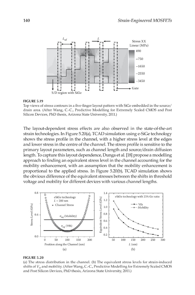
The layout-dependent stress effects are also observed in the state-of-the-art
strain technologies. In Figure 5.20(a), TCAD simulation using e-SiGe technology
shows the stress profile in the channel, with a higher stress level at the edges
and lower stress in the centre of the channel. The stress profile is sensitive to the
primary layout parameters, such as channel length and source/drain diffusion
length. To capture this layout dependence, Dunga et al. [18] propose a modelling
approach to finding an equivalent stress level in the channel accounting for the
mobility enhancement, with an assumption that the mobility enhancement is
proportional to the applied stress. In Figure 5.20(b), TCAD simulation shows
the obvious difference of the equivalent stresses between the shifts in threshold
voltage and mobility for different devices with various channel lengths.
Stress XX
Linear (MPa)
S/D region with SiGe
Gate
L
L sd
490
–750
–1650
–2550
–3450
FIGURE 5.19
Top views of stress contours in a five-finger layout pattern with SiGe embedded in the source/
drain area. (After Wang, C.-C., Predictive Modelling for Extremely Scaled CMOS and Post
Silicon Devices, PhD thesis, Arizona State University, 2011.)
0.8
1.4
1.2
1.0
0.8
0.6
0.4
0.2
0.4
Stress Level (GPa)
Equivalent Stress Level (GPa)
0.0
300
250
200
150
L (nm)
(b)
100
Vth
σ eq (Mobility)
σ eq (Vth)
Mobility
Channel Stress
eSiGe technology with 25% Ge ratio
eSiGe technology
L = 200 nm
50
200
150
Position along the Channel (nm)
(a)
100
50
0
FIGURE 5.20
(a) The stress distribution in the channel. (b) The equivalent stress levels for strain-induced
shifts of V th and mobility. (After Wang, C.-C., Predictive Modelling for Extremely Scaled CMOS
and Post Silicon Devices, PhD thesis, Arizona State University, 2011.)
Strain-Engineered MOSFETs
The layout-dependent stress effects are also observed in the state-of-the-art
strain technologies. In Figure 5.20(a), TCAD simulation using e-SiGe technology
shows the stress profile in the channel, with a higher stress level at the edges
and lower stress in the centre of the channel. The stress profile is sensitive to the
primary layout parameters, such as channel length and source/drain diffusion
length. To capture this layout dependence, Dunga et al. [18] propose a modelling
approach to finding an equivalent stress level in the channel accounting for the
mobility enhancement, with an assumption that the mobility enhancement is
proportional to the applied stress. In Figure 5.20(b), TCAD simulation shows
the obvious difference of the equivalent stresses between the shifts in threshold
voltage and mobility for different devices with various channel lengths.
Stress XX
Linear (MPa)
S/D region with SiGe
Gate
L
L sd
490
–750
–1650
–2550
–3450
FIGURE 5.19
Top views of stress contours in a five-finger layout pattern with SiGe embedded in the source/
drain area. (After Wang, C.-C., Predictive Modelling for Extremely Scaled CMOS and Post
Silicon Devices, PhD thesis, Arizona State University, 2011.)
0.8
1.4
1.2
1.0
0.8
0.6
0.4
0.2
0.4
Stress Level (GPa)
Equivalent Stress Level (GPa)
0.0
300
250
200
150
L (nm)
(b)
100
Vth
σ eq (Mobility)
σ eq (Vth)
Mobility
Channel Stress
eSiGe technology with 25% Ge ratio
eSiGe technology
L = 200 nm
50
200
150
Position along the Channel (nm)
(a)
100
50
0
FIGURE 5.20
(a) The stress distribution in the channel. (b) The equivalent stress levels for strain-induced
shifts of V th and mobility. (After Wang, C.-C., Predictive Modelling for Extremely Scaled CMOS
and Post Silicon Devices, PhD thesis, Arizona State University, 2011.)