

135
Strain-Engineered MOSFETs
simplicity. A thick dielectric hard mask on top of the fin was not included.
It has been observed that the stress profiles are almost identical, except for
a change in sign. The amount of induced stress in the channel depends on
the distance between the capping layer and the fin, which increases toward
the bottom of the fin due to the nonzero thickness of the gate electrode.
Thus, the induced stress profile is nonuniform from the top to the bottom
of the fin. Figure 5.14 shows the mobility enhancement contours in three
directions. Figures 5.15 and 5.16 show the device performance enhancement in the drain current due to stress.
Strain effects on FinFETs have also been studied [10]. The total hole mobility of the FinFET with respect to the stress is shown in Figure 5.17, compared with the single-gate (110)- and (001)-oriented p-type devices at the
inversion charge density of 1 × 10 13 /cm 2 . In the calculation of the single-gate
devices, the doping density is taken to be 1 × 10 17 /cm 3 . This is a low doping
density compared with the contemporary CMOS technology. Even so, the
FinFET shows significantly greater mobility than the bulk devices. If larger
doping density is applied, the mobility advantage of the FinFET would be
even larger. When 3 GPa uniaxial compressive stress is applied to a FinFET,
about 300% enhancement of the mobility is expected, compared to only 200%
enhancement for a bulk (110)-oriented transistor, as shown in Figure 5.18.
Even though the (001)-oriented p-MOSFET shows greater relative enhancement (over 400%), the absolute mobility is still lower than that of the FinFET
due to its low mobility with no stress.
Nitride cap layer
Materials:
SiO~2
Si~3 N~4
Silicon
Polysilicon
(a)
(b)
Gate poly
Si fin
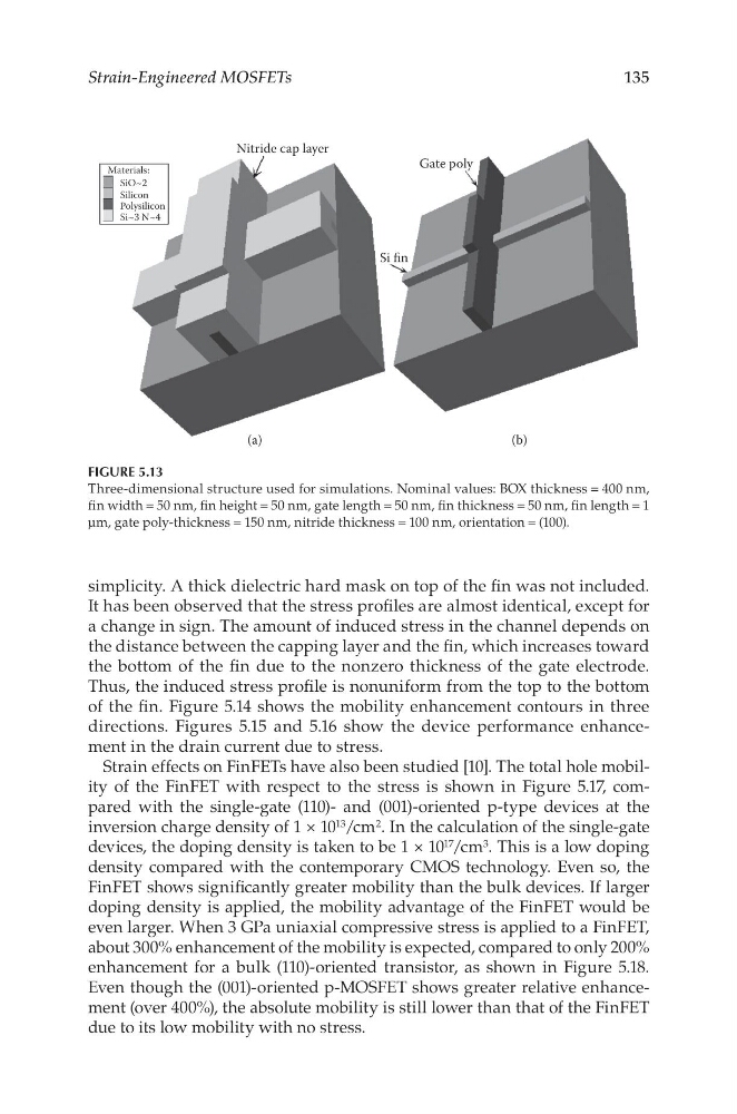
FIGURE 5.13
Three-dimensional structure used for simulations. Nominal values: BOX thickness = 400 nm,
fin width = 50 nm, fin height = 50 nm, gate length = 50 nm, fin thickness = 50 nm, fin length = 1
μm, gate poly-thickness = 150 nm, nitride thickness = 100 nm, orientation = (100).
Strain-Engineered MOSFETs
simplicity. A thick dielectric hard mask on top of the fin was not included.
It has been observed that the stress profiles are almost identical, except for
a change in sign. The amount of induced stress in the channel depends on
the distance between the capping layer and the fin, which increases toward
the bottom of the fin due to the nonzero thickness of the gate electrode.
Thus, the induced stress profile is nonuniform from the top to the bottom
of the fin. Figure 5.14 shows the mobility enhancement contours in three
directions. Figures 5.15 and 5.16 show the device performance enhancement in the drain current due to stress.
Strain effects on FinFETs have also been studied [10]. The total hole mobility of the FinFET with respect to the stress is shown in Figure 5.17, compared with the single-gate (110)- and (001)-oriented p-type devices at the
inversion charge density of 1 × 10 13 /cm 2 . In the calculation of the single-gate
devices, the doping density is taken to be 1 × 10 17 /cm 3 . This is a low doping
density compared with the contemporary CMOS technology. Even so, the
FinFET shows significantly greater mobility than the bulk devices. If larger
doping density is applied, the mobility advantage of the FinFET would be
even larger. When 3 GPa uniaxial compressive stress is applied to a FinFET,
about 300% enhancement of the mobility is expected, compared to only 200%
enhancement for a bulk (110)-oriented transistor, as shown in Figure 5.18.
Even though the (001)-oriented p-MOSFET shows greater relative enhancement (over 400%), the absolute mobility is still lower than that of the FinFET
due to its low mobility with no stress.
Nitride cap layer
Materials:
SiO~2
Si~3 N~4
Silicon
Polysilicon
(a)
(b)
Gate poly
Si fin
FIGURE 5.13
Three-dimensional structure used for simulations. Nominal values: BOX thickness = 400 nm,
fin width = 50 nm, fin height = 50 nm, gate length = 50 nm, fin thickness = 50 nm, fin length = 1
μm, gate poly-thickness = 150 nm, nitride thickness = 100 nm, orientation = (100).