

134
Strain-Engineered MOSFETs
The effects of strain on the performance of FinFETs with {110}/<110> and
{100}/<100> surface orientation/current direction have been investigated [9].
Substrate-induced strain was studied, and it was found that sSOI improves
{110} and {100} electron mobility by 60 and 30%, respectively. Although {110}
hole mobility is degraded by 35%, {100} hole mobility is enhanced by up to
18%. Therefore, sSOI is suggested for performance enhancement of {100}
CMOS FinFETs, or {110} CMOS FinFETs with selective strain relaxation
in p-MOSFETs. A tensile capping layer is expected to provide dramatic
enhancement (>100%) in {100} electron mobility, while a compressive capping
layer is expected to provide a modest amount (<25%) of {110} hole mobility enhancement. Therefore, dual-stress capping layers with hybrid orientations are suggested as a promising performance booster of CMOS FinFETs.
Mobility enhancement is greater for fins with a high aspect ratio (greater
than 1), so that greater performance enhancement is expected for doublegate FET (FinFET) vs. tri-gate FinFET devices.
Figure 5.13 shows the 3D structure used for simulations. The 100 nm
thick SiNx capping layer has a uniform hydrostatic stress of either 1 GPa
(tensile) or –1 GPa (compressive). The bottom surface is the bottom of the
400 nm thick buried oxide. It is assumed that a thin gate oxide layer will
have a negligible effect on the stress transfer from the capping layer to
the channel, and so it was not included in the simulated structure for
3.0 10
–5
Control
Condensed
SiGe S/D
V D = –0.05 V
Control
Condensed
SiGe S/D
2.5×10 –5
2.0×10
–5
Transconductance, G
m (S/µm)
R
tot = 50 mV/I
D,lin (Ω µm)
1.5×10
–5
1.0×10
–5
5.0×10
–6
0.0
1.2×10
4
1.0×10
4
8.0×10
3
6.0×10
3
4.0×10
3
2.0×10
3
0
–1.5 –1.0 –0.5
–3
–2
–1
0
0.0
0.5
Gate Voltage V G – V th (V)
(a)
(b)
Gate Voltage V G (V)
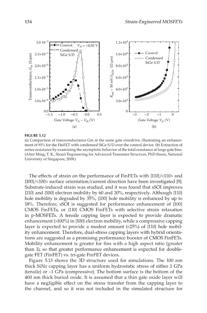
FIGURE 5.12
(a) Comparison of transconductance Gm at the same gate overdrive, illustrating an enhancement of 91% for the FinFET with condensed SiGe S/D over the control device. (b) Extraction of
series resistance by examining the asymptotic behavior of the total resistance at large gate bias.
(After Ming, T. K., Strain Engineering for Advanced Transistor Structure, PhD thesis, National
University of Singapore, 2008.)
Strain-Engineered MOSFETs
The effects of strain on the performance of FinFETs with {110}/<110> and
{100}/<100> surface orientation/current direction have been investigated [9].
Substrate-induced strain was studied, and it was found that sSOI improves
{110} and {100} electron mobility by 60 and 30%, respectively. Although {110}
hole mobility is degraded by 35%, {100} hole mobility is enhanced by up to
18%. Therefore, sSOI is suggested for performance enhancement of {100}
CMOS FinFETs, or {110} CMOS FinFETs with selective strain relaxation
in p-MOSFETs. A tensile capping layer is expected to provide dramatic
enhancement (>100%) in {100} electron mobility, while a compressive capping
layer is expected to provide a modest amount (<25%) of {110} hole mobility enhancement. Therefore, dual-stress capping layers with hybrid orientations are suggested as a promising performance booster of CMOS FinFETs.
Mobility enhancement is greater for fins with a high aspect ratio (greater
than 1), so that greater performance enhancement is expected for doublegate FET (FinFET) vs. tri-gate FinFET devices.
Figure 5.13 shows the 3D structure used for simulations. The 100 nm
thick SiNx capping layer has a uniform hydrostatic stress of either 1 GPa
(tensile) or –1 GPa (compressive). The bottom surface is the bottom of the
400 nm thick buried oxide. It is assumed that a thin gate oxide layer will
have a negligible effect on the stress transfer from the capping layer to
the channel, and so it was not included in the simulated structure for
3.0 10
–5
Control
Condensed
SiGe S/D
V D = –0.05 V
Control
Condensed
SiGe S/D
2.5×10 –5
2.0×10
–5
Transconductance, G
m (S/µm)
R
tot = 50 mV/I
D,lin (Ω µm)
1.5×10
–5
1.0×10
–5
5.0×10
–6
0.0
1.2×10
4
1.0×10
4
8.0×10
3
6.0×10
3
4.0×10
3
2.0×10
3
0
–1.5 –1.0 –0.5
–3
–2
–1
0
0.0
0.5
Gate Voltage V G – V th (V)
(a)
(b)
Gate Voltage V G (V)
FIGURE 5.12
(a) Comparison of transconductance Gm at the same gate overdrive, illustrating an enhancement of 91% for the FinFET with condensed SiGe S/D over the control device. (b) Extraction of
series resistance by examining the asymptotic behavior of the total resistance at large gate bias.
(After Ming, T. K., Strain Engineering for Advanced Transistor Structure, PhD thesis, National
University of Singapore, 2008.)